Printed Circuit Board (PCB) design is a critical skill for engineers, hobbyists, and electronics enthusiasts. PCBs are the backbone of modern electronics, powering everything from simple gadgets to advanced computing systems. Whether you’re designing a PCB for a hobby project or a commercial product, understanding the process is key to creating reliable, cost-effective, and manufacturable boards. This comprehensive guide will walk you through the steps of PCB design, from concept to production, while incorporating SEO-optimized keywords to help you find the information you need.
What is PCB Design?
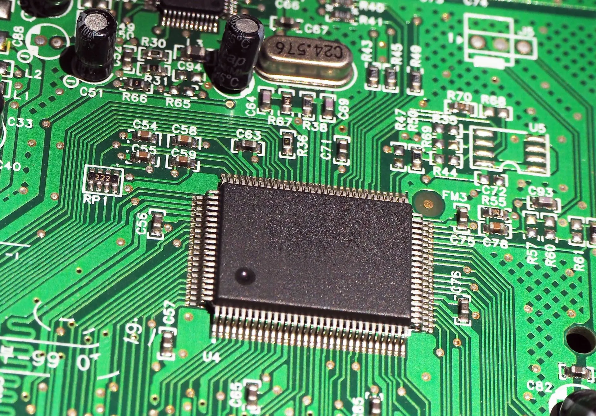
PCB design is the process of creating a layout for an electronic circuit that allows components to be connected via conductive pathways, pads, and traces. It involves transforming a schematic diagram into a physical board that can be manufactured and assembled. A well-designed PCB ensures optimal performance, reduces manufacturing costs, and minimizes the risk of errors.
Define Your Circuit Requirements
Before diving into the PCB design process, clearly outline the requirements of your circuit. Consider the following:
- Functionality: What is the purpose of the circuit?
- Components: What components are needed, and how will they interact?
- Power Requirements: What voltage and current levels are required?
- Size Constraints: What are the physical dimensions of the PCB?
- Environmental Factors: Will the board operate in extreme temperatures, humidity, or mechanical stress?
Defining these parameters early ensures a smoother design process and avoids costly revisions later.
Create a Schematic Diagram
The schematic diagram is the blueprint of your circuit. It visually represents the electrical connections and components. Follow these steps:
- Choose Schematic Capture Software: Popular tools include KiCad (free), Eagle, Altium Designer, and OrCAD.
- Add Components: Place symbols for resistors, capacitors, ICs, and other parts.
- Define Connections: Use wires or nets to connect components logically.
- Assign Values: Specify component values (e.g., resistance, capacitance) and part numbers.
- Follow Best Practices: Ensure the schematic is clear, well-organized, and easy to understand.
A well-drawn schematic is essential for accurate PCB layout design.
Select PCB Design Software
Choosing the right PCB design software is crucial for creating an efficient layout. Here are some popular options:
- KiCad: Free, open-source, and beginner-friendly.
- Eagle: User-friendly with a vast component library.
- Altium Designer: Industry-standard software with advanced features.
- OrCAD: Ideal for professional and complex designs.
Select software that aligns with your skill level and project requirements.
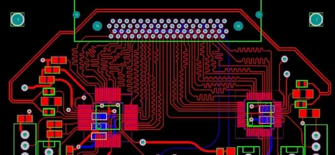
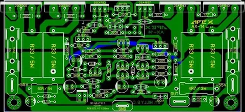
Design the PCB Layout
The PCB layout is where your schematic comes to life. Follow these steps:
- Define Board Dimensions: Set the size and shape based on your enclosure or space constraints.
- Place Components: Arrange components logically to minimize trace lengths and avoid interference.
- Layer Stackup: Decide on the number of layers (single-layer, double-layer, or multi-layer).
- Routing: Connect components using conductive traces. Follow PCB routing techniques like avoiding 90-degree angles and using 45-degree bends.
- Power and Ground Planes: Dedicate layers to power and ground to reduce noise and improve stability.
Proper component placement and routing are critical for signal integrity and manufacturability.
Perform Design Rule Checks (DRC)
Before finalizing the design, run a Design Rule Check (DRC) to identify potential issues. Common checks include:
- Trace Clearance: Ensure adequate spacing between traces.
- Component Overlap: Verify no components are overlapping.
- Unrouted Connections: Confirm all connections are properly routed.
- Hole Sizes: Check that drill holes match component specifications.
DRC helps catch errors early, saving time and money during manufacturing.
Generate Manufacturing Files
Once the design passes DRC, generate the necessary files for manufacturing:
- Gerber Files: Used by manufacturers to produce the PCB.
- Drill Files: Specify hole locations for vias and through-hole components.
- Bill of Materials (BOM): List all components required for assembly.
- Pick and Place File: Provides component placement data for automated assembly.
These files ensure your design is accurately translated into a physical board.
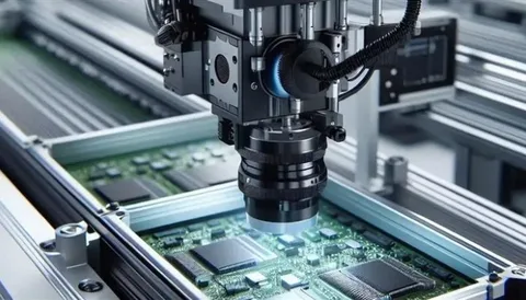
Fabrication and Assembly
Send your Gerber files and BOM to a PCB manufacturer. Options include:
- Prototype Fabrication: For testing and validation.
- Mass Production: For large-scale manufacturing.
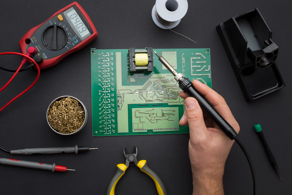
After fabrication, assemble the board using Surface Mount Technology (SMT) or Through-Hole Technology (THT). PCB prototyping is a great way to test your design before full-scale production.
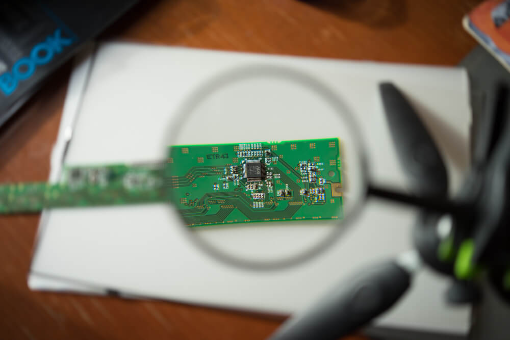
Testing and Debugging
After assembly, thoroughly test the PCB to ensure functionality:
- Visual Inspection: Check for missing or misplaced components.
- Continuity Testing: Verify all electrical connections are intact.
- Power-On Testing: Apply power and measure voltages.
- Functional Testing: Test the board under real-world conditions.
Testing helps identify and resolve issues before the final product is deployed.
Best Practices for PCB Design
- Minimize Trace Lengths: Shorter traces reduce resistance and interference.
- Use Ground Planes: Dedicated ground layers minimize electromagnetic interference (EMI).
- Avoid 90-Degree Bends: Use 45-degree angles to prevent signal reflections.
- Thermal Management: Add thermal relief pads for heat-dissipating components.
- Follow Design Guidelines: Adhere to PCB layout guidelines and best practices for optimal results.
Conclusion
Designing a PCB is a rewarding process that combines creativity and technical expertise. By following this step-by-step guide, you can create efficient, reliable, and manufacturable PCB designs. Whether you’re a beginner or an experienced designer, continuous learning and adherence to best practices will help you master the art of PCB design.
For more tips and tutorials on PCB design, stay tuned to our blog and explore our resources on PCB design software, PCB routing techniques, and PCB prototyping.