As electronic devices continue to shrink in size while growing in functionality, the demand for high-density PCB design has surged. High-Density Interconnect (HDI) PCBs are critical in modern electronics, enabling complex circuits to be incorporated into compact designs. While HDI PCBs provide numerous advantages, they also introduce unique challenges that require innovative solutions.
What is High-Density PCB Design?
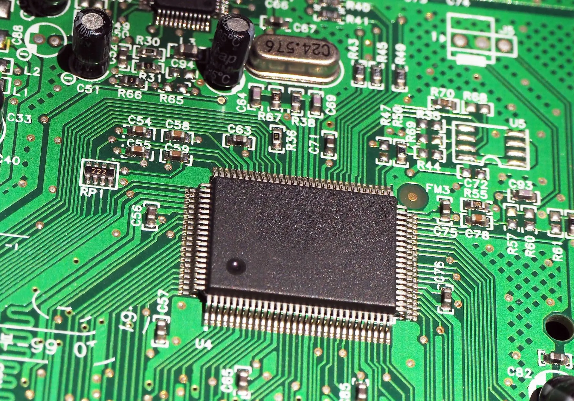
High-density PCB design means the conception of packing more appliances on a single particle board using sophisticated technologies. This includes high-density interconnects that allow for more connections per unit area; this involves increased sizes of vias, increased density of lines and spaces as well as micro vias. HDI PCBs are relevant in communications applications such as smartphones and tablets, portable medical devices, automotive electronics and other applications that require high degrees of integration while being small and lightweight.
Advantages of High-Density PCB Design
Compact Size:
HDI PCBs make it easy for engineers to accommodate more functionality within a confined space within the gadget. High density, therefore, offers the possibility of making mobile, suitcase-sized electronic products through the miniaturization of components and, for example, optimum placement of circuits on boards.
Improved Performance:
Due to the short electrical journey within the highest-density interconnect Printed Circuit Board, signal loss is minimized, signal integrity is improved and the general functionality is boosted. This is particularly important in applications that are likely to be frequent such as 5G, IoT devices and others.
Layer Reduction:
To some extent, rapid HDI PCBs can accomplish complications with fewer layers and cause the manufacturing costs as well as the manufacturing path to become easier.
Lightweight Solutions:
High-density designs help in reducing the weight of devices and thus dvico is good for applications such as drones, wearable and aerospace applications.
Enhanced Reliability:
HDI technology brings less risk of defects and also increases the life period of products using upgraded materials and production techniques.
High Density PCB design application
High-density PCBs are integral to various industries, including:
Consumer Electronics:
Mobile phones, tablets, and laptops all require HDI PCBs because of miniaturization and high performance.
Automotive Industry:
HDI PCBs are a necessity for application-based systems such as ADAS and in-car infotainment systems due to the complexity of their circuits and their reliability.
Medical Devices:
Pacemakers and diagnostic instruments benefit from using the High-Density Interconnection’s (HDI) PCBs due to their size and accuracy.
Aerospace and Defense:
High-quality and lightweight HDI PCBs are crucial in the application of aerospace, satellites and the military.
Some difficulties in designing High-Density PCBs
Complex Manufacturing Processes:
ULM PCBs carry more demanding features that are difficult to develop and produce such as laser drilled microvia and high precision etched features thereby having high technologies.
Thermal Management:
Arranging the components in a compact stack makes heat removal a very difficult problem. Lack of thermal control may often result in unstable operation or damage of some components.
Signal Integrity Issues:
The higher density of traces leads to problems of electromagnetic interference and crosstalk, which reduce the signal quality.
Cost Considerations:
Although they lower the expenses in some aspects, the integrated manufacturing methods and materials of the HDI PCB surpass the other kinds of circuit board.
Design Limitations:
Low variability and high density impose certain restrictions on the design concept, therefore calling for sophisticated equipment and a high skill level.
PCB Design Issues in High-Density Design
As a brief, addressing thermal management in dense designs can be best termed as challenging.
Thermal vias, heat sinks, and other new materials minimize heat problems in high-density PDC designs.
Controlling or preventing Signal Integrity problems
By differential pair routing, controlling impedance, and the use of ground planes EMI and crosstalk are minimized.
How Technology Can Solve HDI PCB Issues
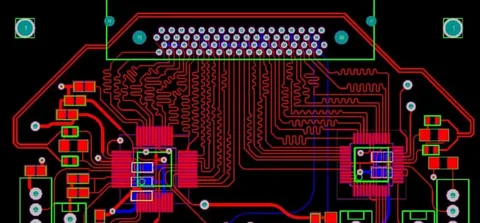
Advanced Design Software:
The current CAD systems allow engineers to draw complicated HDI PCBs with a high degree of accuracy in terms of performance and fabrication.
Laser Drilling and Microvia Technology:
These techniques enable the formation of connections suitable for higher component density and smaller and more accurate control.
Material Innovations:
The laminates and substrate with high operating speeds enhance heat dissipation and minimize signal attenuation.
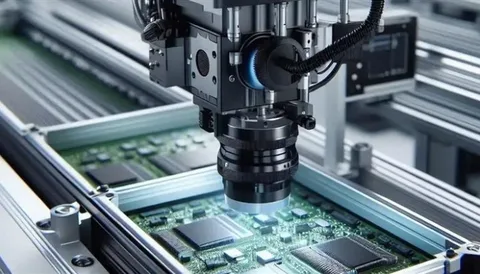
Automated Testing and Inspection:
Automated optical inspection (AOI) and X-ray examination guarantee the quality and reliability of HDI PCBs, decreasing the defects and the related decrease in production speed.
Benefits vs. Challenges: Finding the Balance
Of course, designing at such density levels poses some issues but the advantages are many times worth the effort if handled appropriately. That is why the most important element is the innovation of tactics with performance and cost in the union of design and manufacturing teams.
The Future of High-Density PCB Design
Overall, the need for HDI PCBs will remain intact predominantly credited to ever-evolving technology. New patterns such as the 5G connection, artificial intelligence, and IoT gadgets are the demands for even tinier, quicker, and more effective circuit boards. Future developments such as the affordable high-density interconnect PCB ( HDI) and the additive manufacturing technology will serve to enhance the high-density designs.
Conclusion
High-density PCB design is one of the fundamental key components of efficient electronics where smaller devices are built to pack more and more functionality into smaller and smaller packages. Thermal management, signal integrity, and manufacturing are the primary limitations of HDI PCBs, but the compactness, reliability, and performance of PCBs are essential in the modern technological setting.
These challenges, however, can be addressed by adopting more sophisticated technology and powerful strategic approaches that will enable the companies to make the most out of HDI PCBs as they help enhance the products offered in the market which is deemed to be highly competitive.