A Printed Circuit Board (PCB) is the backbone of virtually every electronic device—from smartphones and computers to medical equipment and automotive systems. Whether you’re an electronics hobbyist, a student, or a professional engineer, understanding the essential components and processes involved in PCB creation is crucial. This guide will walk you through the fundamental requirements for making a PCB, from design to assembly.
Understanding the Basics of a Printed Circuit Board
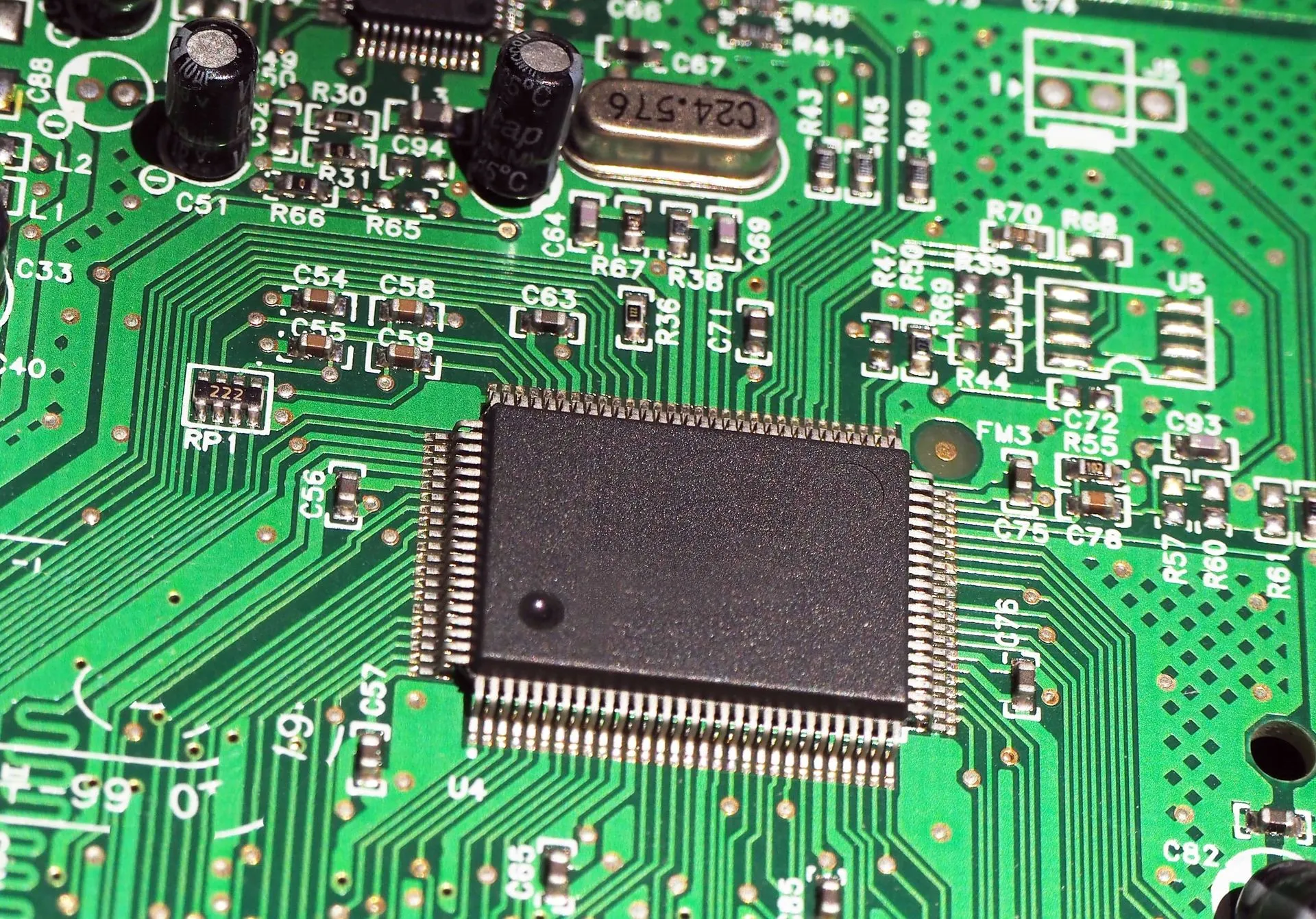
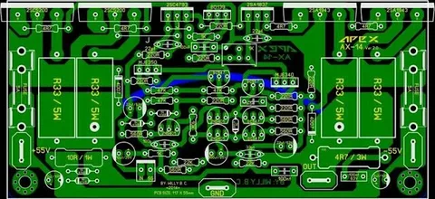
At its core, a PCB is a flat board made of insulating material, typically fiberglass, with conductive pathways etched onto its surface. These pathways, or traces, connect various electronic components, allowing them to communicate and function together. The primary purpose of a Printed Circuit Board is to provide mechanical support and electrical connections for electronic components.
Essential Components Needed for PCB Manufacturing
Creating a Printed Circuit Board involves several key materials and tools:
Copper-Clad Laminate (CCL)
This is the base material for the PCB, consisting of a non-conductive substrate (like fiberglass) coated with a thin layer of copper. The copper layer is where the circuit traces are etched.
Photoresist Material
A light-sensitive chemical applied to the copper surface. It hardens when exposed to ultraviolet (UV) light, allowing for the creation of intricate circuit patterns.
Etching Solution
A chemical solution, often ferric chloride or ammonium persulfate, used to remove the unexposed copper, leaving behind the desired circuit traces.
Drill Bits
Used to create holes for through-hole components and vias (electrical connections between layers).
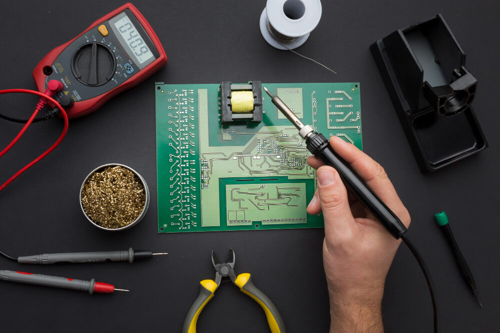
Soldering Equipment
Includes soldering irons, soldering wire, and flux, essential for attaching components to the PCB.
PCB Design Software
Tools like Eagle, KiCad, or Altium Designer are used to design the circuit layout and generate the necessary files for manufacturing.
The PCB Manufacturing Process
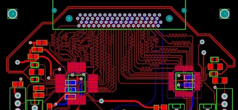
Designing the Circuit
Using Printed Circuit Board design software, you create a schematic diagram of your circuit, placing components and defining their connections. This design is then converted into a layout, specifying the physical placement of components and routing of traces.
Printing the Design
The layout is printed onto a transparent film, which will be used as a mask during the exposure process.
Preparing the Copper-Clad Laminate
The CCL is cleaned and coated with a layer of photoresist material.
Exposure
The printed design is aligned with the CCL, and UV light is exposed to the assembly. The areas not covered by the design harden, while the exposed areas remain soft.
Developing
The unexposed photoresist is washed away, revealing the copper beneath.
Etching
The CCL is immersed in an etching solution, removing the unprotected copper and leaving behind the circuit traces.
Drilling
Holes are drilled for component leads and vias.
Solder Mask Application
A protective layer is applied to prevent solder bridges and protect the traces.
Silkscreen Printing
Labels and component identifiers are printed onto the PCB.
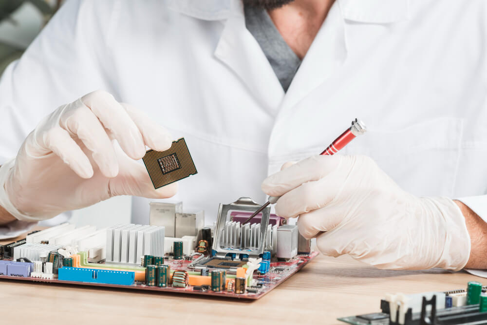
Soldering Components
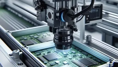
Components are placed onto the PCB and soldered into place, either manually or using automated machines.
Testing and Quality Control
After assembly, the Printed Circuit Board undergoes various tests to ensure functionality:
- Visual Inspection: Checking for obvious defects like solder bridges or misaligned components.
- Automated Optical Inspection (AOI): Machines scan the PCB for defects that might not be visible to the naked eye.
- Functional Testing: Verifying that the PCB performs as intended under operational conditions.
Tools and Equipment for PCB Fabrication
Depending on the scale and complexity of your PCB project, you might need the following tools:
- Laser Printer: For printing the design onto transfer paper.
- Iron or Laminator: To transfer the design onto the copper surface.
- UV Light Box: For exposing the photoresist material.
- Etching Tank: For immersing the PCB in the etching solution.
- Drill Press: For precise drilling of holes.
- Soldering Station: For attaching components.
Safety Considerations
Working with PCBs involves handling chemicals and hot equipment. Always wear appropriate safety gear, including gloves and goggles. Work in a well-ventilated area, and follow all safety instructions provided with chemicals and equipment.
Alternative Methods for PCB Production
For those without access to traditional PCB fabrication tools, alternative methods include:
- Inkjet Printing: Using conductive ink to print circuits directly onto substrates.
- Laser Etching: Employing a laser to etch the circuit design onto the copper surface.
- Outsourcing: Sending your design files to a PCB manufacturer for professional fabrication.
Conclusion
Creating a Printed Circuit Board is a multifaceted process that combines design, chemistry, and precision engineering. Whether you’re crafting a simple project at home or developing complex electronics for commercial use, understanding the materials, tools, and steps involved is essential. By following this guide, you can embark on your PCB creation journey with confidence, ensuring your electronic projects are both functional and reliable.