In the realm of electronics manufacturing, the integrity of solder joints is paramount. A crucial step in ensuring this integrity is solder paste inspection (SPI). This process verifies that the solder paste has been accurately applied to the printed circuit board (PCB), setting the foundation for reliable and durable electronic assemblies.
What Is Solder Paste Inspection?
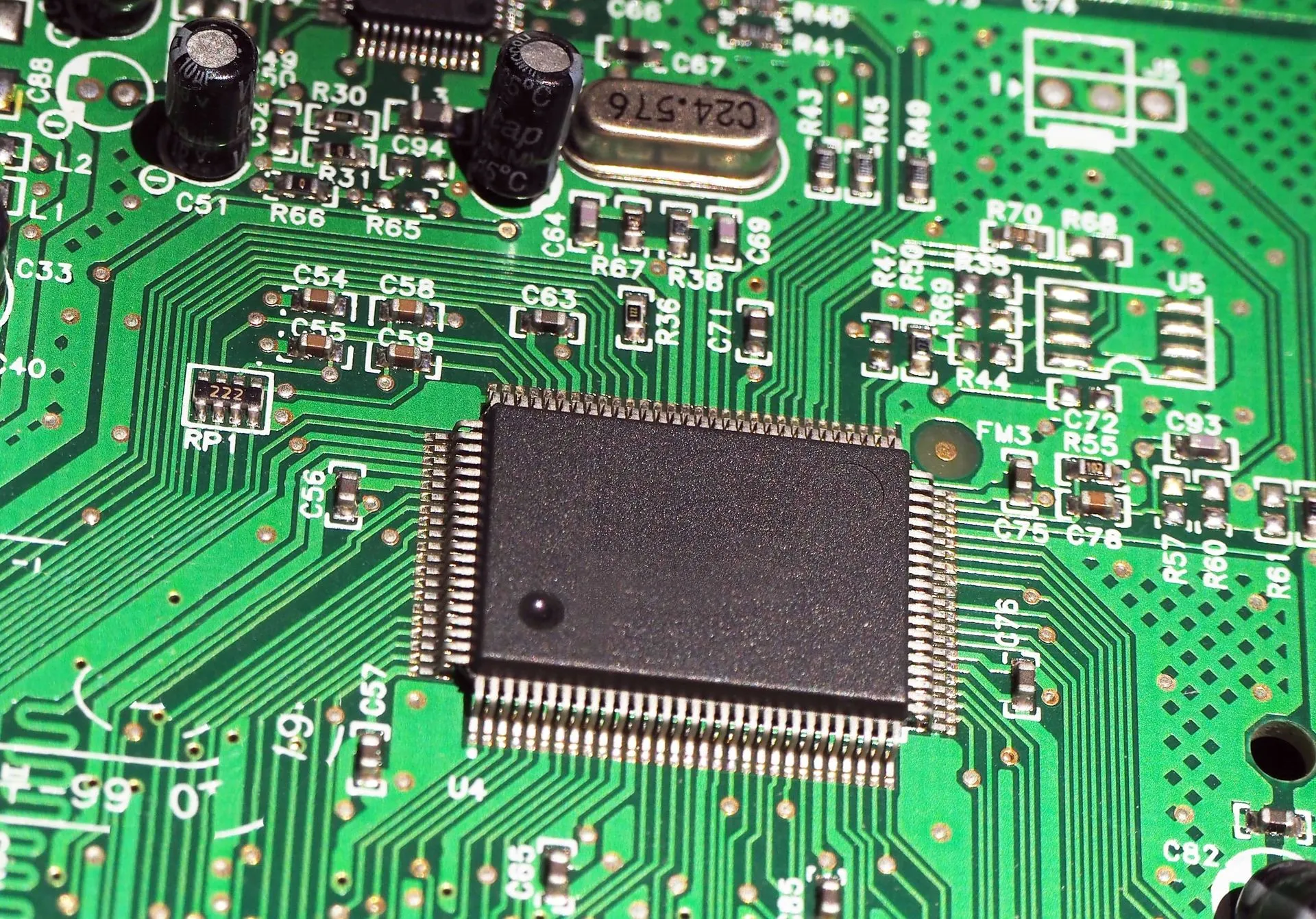
Solder paste inspection is a quality control procedure employed during the surface-mount technology (SMT) assembly process. It involves assessing the application of solder paste onto a PCB to ensure it meets specific criteria such as volume, alignment, and consistency. This inspection is vital because improper solder paste application can lead to defects like insufficient solder joints, bridging, or misalignment, which compromise the functionality and reliability of the final product.
The Importance of Solder Paste Inspection
Defect Prevention
Early detection of solder paste application issues allows manufacturers to address problems before they escalate into more significant defects. This proactive approach minimizes the risk of costly rework and ensures a higher yield of functional PCBs.
Enhanced Reliability
By ensuring that solder paste is applied correctly, SPI contributes to the formation of strong and reliable solder joints. This leads to improved electrical and mechanical performance of the assembled PCB, reducing the likelihood of failures in the field.
Cost Efficiency
Identifying and rectifying solder paste application issues early in the assembly process reduces waste and the need for rework. This not only saves time and resources but also lowers production costs, contributing to the overall profitability of the manufacturing process.
Techniques and Technologies in Solder Paste Inspection
2D Solder Paste Inspection
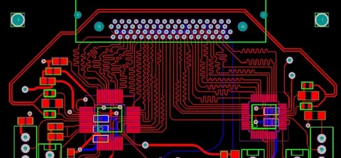
Traditional 2D SPI systems utilize high-resolution cameras to capture top-down images of the PCB. These images are analyzed to assess parameters like area coverage and alignment. While effective for detecting certain defects, 2D systems have limitations in measuring the volume and height of solder paste deposits.
3D Solder Paste Inspection
Advancements in technology have led to the development of 3D SPI systems, which employ optical sensors and laser triangulation to create detailed topographical maps of solder paste deposits. These systems can measure the volume, height, and shape of the solder paste, allowing for more accurate detection of defects such as insufficient paste, excessive paste, and misalignment.
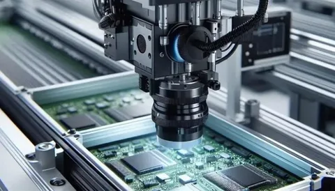
Automated Optical Inspection (AOI)
AOI systems are integrated into the SPI process to provide an additional layer of inspection. These systems use high-resolution cameras and specialized software to compare real-time images of the PCB with predefined templates, identifying defects like missing components, polarity errors, and misalignment. The feedback from AOI systems allows for immediate adjustments, streamlining the inspection process.
Automated X-ray Inspection (AXI)

For more complex assemblies, especially those with components like ball grid arrays (BGAs), AXI technology is employed. AXI uses X-rays to visualize hidden areas, such as solder joints under BGAs, detecting issues like voids within solder joints, tilted BGAs, and missing balls in BGA components. This technique provides a grayscale image, revealing internal defects based on molecular density differences.
Common Defects Detected by Solder Paste Inspection
- Insufficient Paste: Occurs when too little solder paste is applied, leading to weak or open solder joints.
- Excessive Paste: Too much solder paste can cause bridging between pads, leading to short circuits.
- Misalignment: Solder paste applied off-center can result in poor component placement and unreliable solder joints.
- Tombstoning: A defect where one side of a component lifts off the PCB during reflow due to uneven solder paste application.
- Solder Smearing: Occurs when solder paste spreads beyond the intended area, potentially causing shorts.
Implementing Solder Paste Inspection in the Manufacturing Process
Integration with SMT Lines
SPI systems are integrated into the SMT assembly line, allowing for real-time inspection of solder paste deposits on multiple PCBs with high speed and precision. This integration ensures that any defects are detected early, minimizing disruptions to the production process.
Data Collection and Analysis
Modern SPI systems collect and analyze vast amounts of data during the inspection process. This data provides valuable insights into the solder paste application process, helping manufacturers identify trends and recurring issues. By analyzing this data, manufacturers can make informed adjustments to improve the quality and efficiency of the assembly process.
Continuous Improvement
The feedback provided by SPI systems supports continuous improvement initiatives. By regularly reviewing inspection data and making necessary adjustments, manufacturers can enhance the consistency and reliability of their solder paste application, leading to higher-quality PCBs and reduced defect rates.
Conclusion
Solder paste inspection is a critical component of quality control in PCB assembly. By employing advanced inspection technologies and integrating them into the manufacturing process, manufacturers can ensure the accurate application of solder paste, leading to reliable and high-quality electronic assemblies. The benefits of SPI extend beyond defect detection, contributing to cost efficiency, enhanced reliability, and continuous improvement in the manufacturing process.