The PCB Manufacturing Process is a complex and precise series of steps that transform a conceptual electronic design into a functional printed circuit board (PCB). Whether you’re a novice in electronics or a seasoned engineer, understanding this process is crucial for designing reliable and efficient electronic devices.
What Is a PCB?
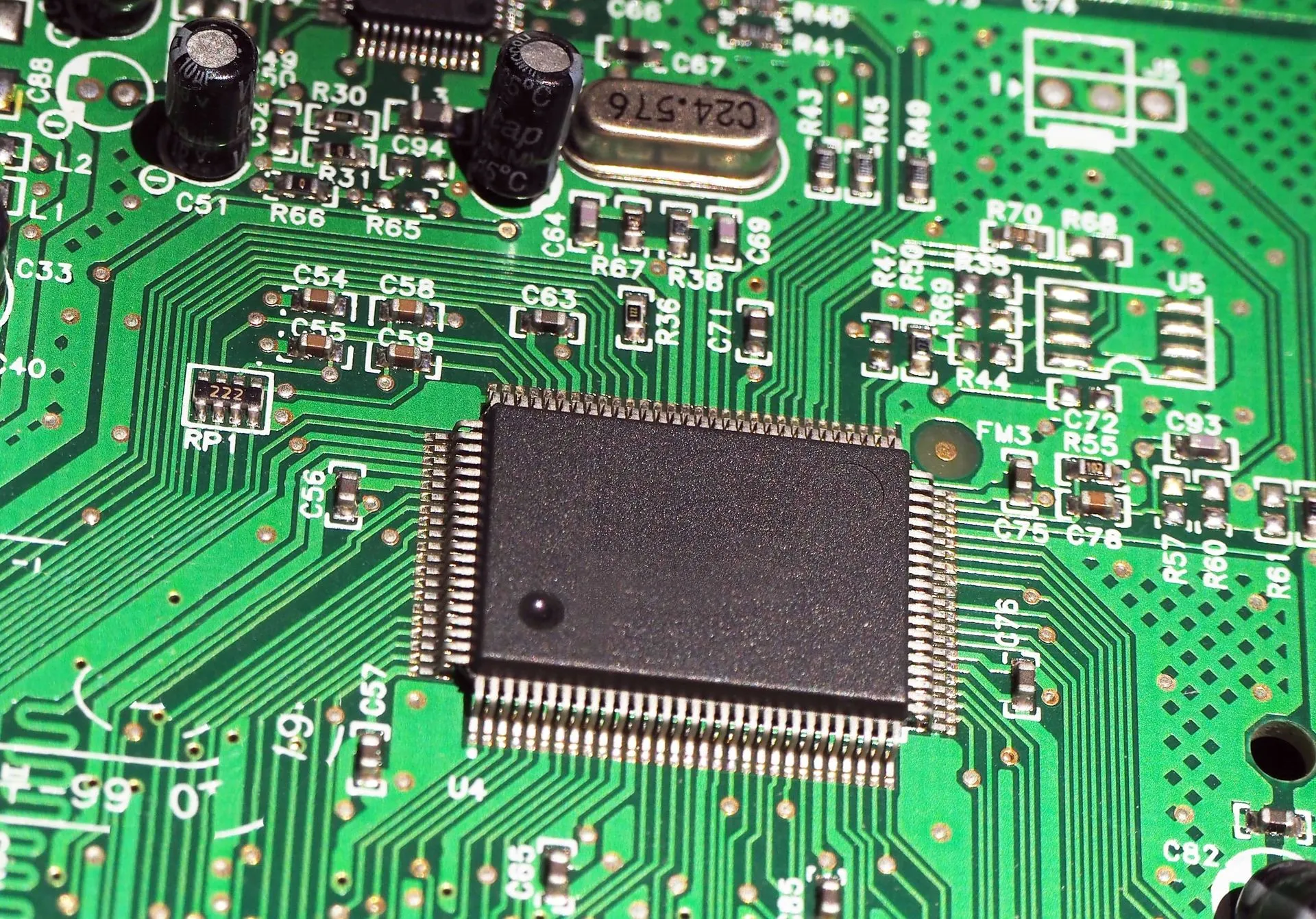
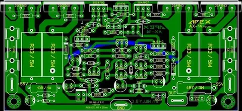
A Printed Circuit Board (PCB) is a flat board made of insulating material, typically fiberglass, with conductive pathways etched onto its surface. These pathways, made of copper, connect various electronic components like resistors, capacitors, and integrated circuits, allowing them to communicate electrically.
The PCB Manufacturing Process: An Overview
The PCB Manufacturing Process involves several key stages, each critical to ensuring the final product meets the desired specifications and quality standards. Here’s a detailed look at each step:
Design and Schematic Creation
The process begins with the creation of a schematic diagram, which outlines the electrical connections between components. Engineers use specialized software tools to design the circuit, ensuring all components are correctly placed and connected. This design is then converted into a PCB layout.
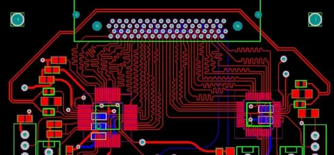
PCB Layout and Gerber File Generation
In this stage, the schematic is translated into a physical layout, specifying the placement of components and routing of electrical traces. The design is checked for errors and manufacturability. Once finalized, Gerber files are generated. These files contain all the information needed for the PCB fabrication process, including layer definitions, drill data, and component placements.
Printing Inner Layers
For multi-layer PCBs, the inner layers are printed first. A copper-clad laminate is coated with a photosensitive material. The Gerber files are used to expose the copper to UV light, transferring the circuit pattern onto the laminate. The exposed areas are then etched away, leaving behind the desired copper traces.
Layer Alignment and Lamination
After the inner layers are prepared, they are stacked together with insulating layers, known as prepreg, in between. This stack is then heated and pressed in a lamination process, bonding the layers into a single, solid board. This step is crucial for multi-layer PCBs to ensure proper alignment and adhesion.
Drilling
Once the laminate is solidified, holes are drilled into the PCB for vias (vertical interconnects) and component leads. These holes are essential for connecting different layers and for mounting components. The drilling process requires high precision to ensure the holes are correctly placed and of the right size.
Plating and Etching
The drilled holes are then plated with a thin layer of copper to create electrical connections between layers. This is followed by an etching process, where unwanted copper is removed, leaving behind the desired circuit pattern. This step defines the electrical pathways on the PCB.
Solder Mask Application
A solder mask, typically green, is applied to the PCB to protect the copper traces and prevent solder bridges during component soldering. The mask also defines the areas where components will be mounted.
Silkscreen Printing
The silkscreen layer is printed onto the PCB to label component designators, logos, and other markings. This helps in identifying components during assembly and provides necessary information for assembly and troubleshooting.
Surface Finish
To ensure good solderability and protect the copper pads, a surface finish is applied. Common finishes include Hot Air Solder Leveling (HASL), Electroless Nickel Immersion Gold (ENIG), and Immersion Silver. Each finish has its advantages and is chosen based on the specific requirements of the PCB.
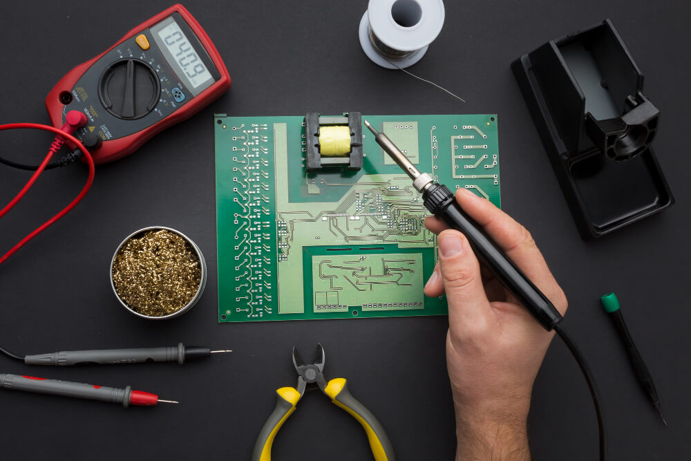
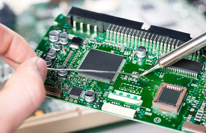
Electrical Testing
Before moving to assembly, the PCB undergoes electrical testing to check for shorts, opens, and other defects. This step ensures that the board is electrically sound and ready for component placement.
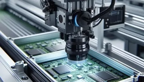
Final Inspection and Quality Control
The final PCB is inspected for visual defects, such as misalignment, solder mask issues, or silkscreen errors. Automated Optical Inspection (AOI) systems are often used to detect these defects with high precision.
Importance of the PCB Manufacturing Process
Understanding the PCB Manufacturing Process is vital for several reasons:
- Design Optimization: Knowledge of the manufacturing steps allows designers to create PCBs that are easier and more cost-effective to produce.
- Quality Assurance: Awareness of potential pitfalls in the process helps in identifying and mitigating defects early.
- Cost Efficiency: Streamlining the manufacturing process can lead to significant cost savings, especially in large-scale production.
Challenges in PCB Manufacturing
The PCB Manufacturing Process is not without its challenges. Some common issues include:
- Design Errors: Mistakes in the schematic or layout can lead to functional failures.
- Material Defects: Imperfections in the base materials can affect the performance and reliability of the PCB.
- Manufacturing Variations: Variations in the manufacturing process can lead to inconsistencies in the final product.
Addressing these challenges requires careful planning, rigorous testing, and continuous improvement in manufacturing techniques.
Conclusion
The PCB Manufacturing Process is a detailed and intricate journey from initial design to a fully functional finished product. Each step—from schematic creation to final inspection—plays a critical role in ensuring the performance, reliability, and longevity of the printed circuit board. Understanding these stages empowers engineers, designers, and manufacturers to create higher-quality electronics, reduce production costs, and minimize errors.
At Qual-Pro, we specialize in delivering precision-engineered PCBs through a streamlined and highly controlled manufacturing process. Our commitment to quality, innovation, and reliability ensures that every board we produce meets the highest industry standards. Whether you’re building prototypes or scaling for mass production, Qual-Pro is your trusted partner for dependable, high-performance PCB solutions.