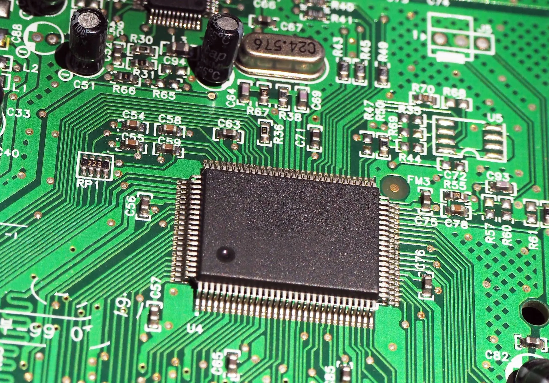
Printed Circuit Boards (PCBs) are the backbone of modern electronics, serving as the foundation for connecting and supporting electronic components. The design of a PCB is crucial, and one of the most significant aspects is its layer structure. Understanding the differences in PCB layer designs—single, double, and multilayer—is essential for selecting the appropriate type for specific applications.
What Are PCB Layer Designs?
PCB layer designs refer to the number and arrangement of conductive and insulating layers within a PCB. These layers determine the board’s complexity, functionality, and suitability for various electronic applications.
Single-Layer PCBs
Single-layer PCBs, also known as single-sided PCBs, consist of a single layer of conductive material (usually copper) on one side of a non-conductive substrate. Components are mounted on the top surface, and all electrical connections are made on this single layer.
Advantages:
- Cost-Effective: Ideal for simple, low-cost applications.
- Easy to Manufacture: Straightforward production process.
- Suitable for Low-Density Circuits: Best for basic electronic devices.
Disadvantages:
- Limited Component Density: Not suitable for complex circuits.
- Higher Risk of Signal Interference: Lack of dedicated ground planes can lead to noise issues.
Common Applications:
- Consumer electronics with minimal complexity.
- Basic LED lighting circuits.
- Simple household appliances.
Double-Layer PCBs
Double-layer PCBs feature conductive layers on both sides of the substrate, allowing components to be mounted on both surfaces. Vias (vertical electrical connections) are used to connect the two layers.
Advantages:
- Increased Component Density: More components can be placed within the same area.
- Better Signal Routing: Allows for more complex circuit designs.
- Improved Performance: Reduced signal interference compared to single-layer PCBs.
Disadvantages:
- More Complex Manufacturing: Requires additional processes like via drilling and plating.
- Higher Cost: More expensive than single-layer PCBs.
Common Applications:
- Industrial control systems.
- Automotive electronics.
- Power supplies.
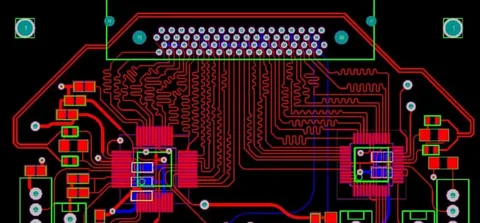
Multilayer PCBs
Multilayer PCBs consist of three or more conductive layers separated by insulating materials. These boards are laminated together to form a single, compact unit. Multilayer PCBs can have 4, 6, 8, or more layers, depending on the complexity of the circuit.

Advantages:
- High Component Density: Accommodates complex circuits in a compact space.
- Enhanced Signal Integrity: Dedicated power and ground planes reduce noise and interference.
- Superior Performance: Suitable for high-speed and high-frequency applications.
Disadvantages:
- High Manufacturing Cost: Complex production processes increase costs.
- Longer Lead Times: More time required for fabrication.
- Design Complexity: Requires advanced design skills and tools.
Common Applications:
- Smartphones and tablets.
- Medical devices.
- Aerospace and defense electronics.
Comparing PCB Layer Designs
| Feature | Single-Layer PCB | Double-Layer PCB | Multilayer PCB |
|---|---|---|---|
| Cost | Low | Moderate | High |
| Manufacturing Complexity | Simple | Moderate | Complex |
| Component Density | Low | Moderate | High |
| Signal Integrity | Basic | Good | Excellent |
| Size Constraints | Less Compact | More Compact | Highly Compact |
| EMI Shielding | None | Limited | Excellent |
| Typical Applications | Basic electronics | Consumer electronics | High-performance devices |
Choosing the Right PCB Layer Design
Selecting the appropriate PCB layer design depends on several factors, including the complexity of the circuit, performance requirements, size constraints, and budget.
- Single-Layer PCBs are suitable for simple, low-cost applications where space is not a significant constraint.
- Double-Layer PCBs offer a balance between cost and performance, making them ideal for moderately complex circuits.
- Multilayer PCBs are necessary for high-performance applications requiring compact designs and superior signal integrity.
Conclusion
Understanding the key differences in PCB layer designs is crucial for selecting the right type of Printed Circuit Boards for your application. Each design offers unique advantages and is suited to specific needs. By considering factors such as complexity, performance, size, and cost, you can make an informed decision that ensures the success of your electronic project.