Efficient PCB component placement is a cornerstone of high-quality electronic design. Mastering this skill not only enhances the functionality and reliability of your circuits but also streamlines the manufacturing process. This guide delves into the principles and best practices of PCB component placement, providing you with the knowledge to optimize your designs.
Understanding PCB Component Placement
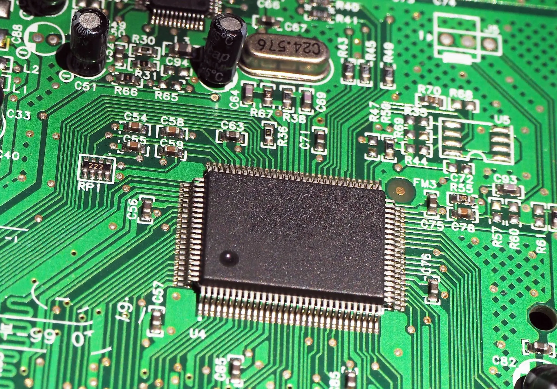
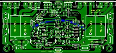
PCB component placement refers to the strategic positioning of electronic components on a printed circuit board. This process is crucial as it directly impacts the board’s performance, manufacturability, and cost-effectiveness. Proper placement ensures minimal signal interference, efficient thermal management, and ease of assembly.
Best Practices for Efficient PCB Component Placement
- Functional Grouping Begin by grouping components based on their functions. For instance, place power supply components like voltage regulators and capacitors near the power input. Similarly, keep analog and digital components separate to minimize noise interference.
- Minimize Trace Lengths Shorter traces reduce resistance and inductance, leading to improved signal integrity. Position components that frequently communicate with each other close together to minimize trace lengths.
- Thermal Management High-power components generate heat, which can affect nearby sensitive components. Place heat-generating components away from heat-sensitive ones and consider using thermal vias or heat sinks to dissipate heat effectively.
- Orientation Consistency Maintain a consistent orientation for components, especially polarized ones like diodes and capacitors. This practice simplifies assembly and reduces the risk of errors.
- Adequate Spacing Ensure sufficient spacing between components to facilitate soldering and prevent short circuits. The recommended spacing varies depending on the component size and type.
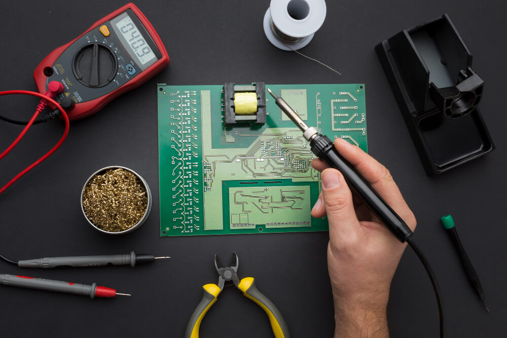
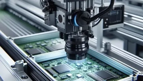
- Design for Manufacturability Consider the capabilities of your PCB manufacturer when placing components. Ensure that components are within the reach of pick-and-place machines and that there is adequate space for automated optical inspection.
- Test Point Accessibility Include test points in your design for easy access during debugging and quality control. Position them in accessible locations without obstructing other components.
- Signal Integrity Considerations For high-speed circuits, maintain controlled impedance and minimize trace lengths. Use ground planes and decoupling capacitors to reduce noise and ensure stable signal transmission.
How PCB Component Placement Affects Performance
Proper PCB component placement goes beyond just fitting parts onto a board. It plays a vital role in determining the circuit’s:
- Signal Integrity
- Power Efficiency
- Thermal Management
- Noise Reduction
- Mechanical Durability
For example, high-frequency components that are placed too far apart can introduce unwanted electromagnetic interference (EMI). Similarly, placing power components near signal-sensitive ICs can compromise data accuracy. Thoughtful placement minimizes these risks, ensuring optimal performance.
Another aspect is electromagnetic compatibility (EMC). Poor placement can lead to EMI, which not only affects your own device but can interfere with nearby systems. Using ground planes, shielding techniques, and isolating analog/digital sections can significantly improve performance.
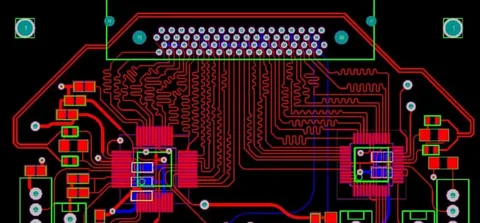
Tools and Techniques for PCB Component Placement
Utilizing advanced PCB design software can significantly enhance the component placement process. These tools offer features like:
- Design Rule Checks (DRC): Automatically identify and correct potential issues in component placement.
- Thermal Simulation: Predict and manage heat distribution across the PCB.
- Signal Integrity Analysis: Assess and optimize signal paths to prevent interference.
- 3D Visualization: View the PCB in three dimensions to detect potential mechanical conflicts.
By leveraging these tools, you can create more efficient and reliable PCB layouts.
Advanced Tips for Efficient PCB Component Placement
As you gain experience, consider these advanced techniques:
Use Hierarchical Design
Break down your schematic into modules and apply the same modular approach to component placement. It helps in troubleshooting and future upgrades.
Consider Serviceability
Place connectors, test points, and frequently replaced components (like fuses) near the edge of the board or in accessible locations.
Simulate First
Use simulation tools integrated into PCB design software to test your layout before prototyping. Simulations can reveal thermal hotspots, signal integrity issues, and layout inefficiencies.
Review and Iterate
Don’t rush your final placement. After your initial layout, take a break and review it again. You might spot improvements in trace routing, airflow, or EMI shielding.
Common Mistakes to Avoid
- Overcrowding Components: Placing components too close together can lead to difficulty in soldering and increased risk of short circuits.
- Ignoring Thermal Effects: Failing to account for heat dissipation can result in component failure.
- Neglecting Signal Integrity: Improper routing can cause signal degradation and interference.
- Inconsistent Orientation: Misaligned components can complicate assembly and increase error rates.
- Lack of Test Points: Omitting test points can hinder debugging and quality control processes.
Conclusion
Efficient PCB component placement is a critical skill that influences the overall success of your electronic designs. By adhering to best practices and utilizing advanced design tools, you can optimize your PCB layouts for performance, reliability, and manufacturability. Remember, thoughtful component placement not only enhances the functionality of your circuits but also contributes to a smoother and more cost-effective production process.