In the realm of modern electronics manufacturing, ensuring the integrity and reliability of printed circuit boards (PCBs) is paramount. As devices become increasingly compact and complex, traditional manual inspection methods struggle to meet the demands for speed, accuracy, and scalability. Enter Automated Optical Inspection (AOI)—a transformative technology that has revolutionized PCB quality control. This article delves into the significance of AOI services, highlighting their role in enhancing PCB quality, optimizing manufacturing processes, and driving cost efficiencies.
Understanding Automated Optical Inspection (AOI)
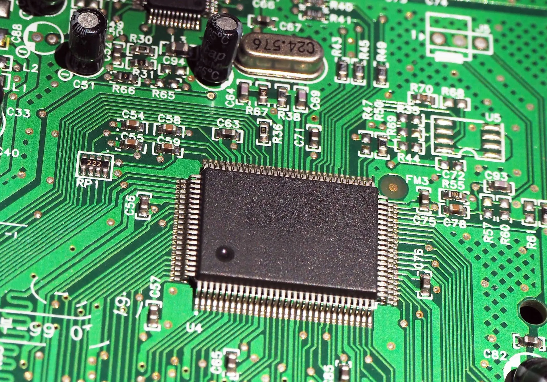
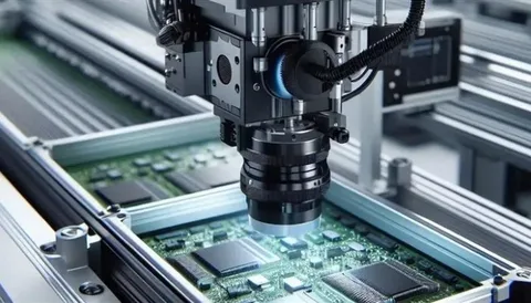
Automated Optical Inspection is a non-contact, high-speed inspection technique that employs advanced imaging systems to detect defects on PCBs. Utilizing high-resolution cameras and sophisticated algorithms, AOI systems capture detailed images of PCB assemblies and compare them against predefined standards. This process enables the identification of various defects, including:
- Misaligned components
- Solder bridges
- Missing components
- Component polarity errors
- Open or short circuits
By automating the inspection process, AOI significantly reduces human error, enhances repeatability, and accelerates the detection of potential issues, ensuring that only high-quality PCBs proceed through the manufacturing pipeline.
The Role of Automated Optical Inspection in Enhancing PCB Quality
Early Detection of Defects
One of the primary advantages of AOI is its ability to detect defects at the earliest stages of the manufacturing process. By identifying issues such as misplacements or soldering defects promptly, manufacturers can address problems before they propagate, reducing the likelihood of defective products reaching the market.
Increased Inspection Speed and Throughput
AOI systems can inspect thousands of components per minute, far surpassing the capabilities of manual inspection. This high throughput ensures that large volumes of PCBs are inspected efficiently, meeting the demands of high-volume production lines without compromising on quality.
Consistency and Repeatability
Unlike human inspectors, AOI systems are not susceptible to fatigue or variability in performance. Their consistent operation ensures uniform inspection quality across all units, leading to a higher level of product consistency and reliability.
Advantages of Implementing AOI in PCB Manufacturing
Cost Efficiency
While the initial investment in AOI equipment can be substantial, the long-term savings are significant. Early detection of defects reduces rework costs, minimizes material waste, and decreases the likelihood of product returns. Over time, these savings offset the initial expenditure, making AOI a cost-effective solution for PCB manufacturers.
Enhanced Process Control and Traceability
Modern AOI systems offer data logging capabilities, capturing detailed information about each inspected PCB. This data provides valuable insights into the manufacturing process, allowing for trend analysis and identification of recurring issues. Such traceability supports continuous improvement initiatives and aids in maintaining compliance with industry standards.
Scalability for Diverse Production Needs
AOI systems are adaptable to various production scales, from small-batch prototypes to large-scale manufacturing. Their flexibility allows manufacturers to maintain high-quality standards across different production volumes, ensuring that quality is not compromised regardless of batch size.

Challenges and Considerations in AOI Implementation
High Initial Setup Costs
The acquisition and installation of AOI systems involve significant upfront costs, which can be a barrier for smaller manufacturers. However, as previously discussed, the long-term benefits often outweigh these initial expenses.
Complexity in Programming for New Designs
Each new PCB design may require reprogramming of the AOI system to accommodate different component placements and layouts. This process can be time-consuming and may require specialized expertise.
Limitations in Detecting Internal Defects
While AOI excels at identifying surface-level defects, it may not detect issues within the internal layers of a PCB, such as voids or misalignments in multi-layer boards. Complementary inspection methods, like X-ray inspection, may be necessary for comprehensive quality assurance.
The Future of AOI in PCB Manufacturing
As technology advances, so do the capabilities of Automated Optical Inspection systems. Future developments may include:
- Integration with Artificial Intelligence (AI): AI algorithms can enhance defect detection accuracy by learning from vast datasets and improving over time.
- 3D Imaging: 3D AOI systems can provide more detailed inspections, especially for complex component geometries.
- Real-time Feedback: Immediate feedback from AOI systems can enable on-the-fly adjustments in the manufacturing process, further enhancing quality control.
Conclusion
Automated Optical Inspection stands at the forefront of quality assurance in PCB manufacturing. By offering rapid, consistent, and accurate defect detection, AOI services play a crucial role in producing high-quality PCBs that meet the stringent demands of modern electronics. While challenges exist, the advantages of implementing AOI far outweigh the drawbacks, making it an indispensable tool for manufacturers aiming to maintain competitiveness and deliver reliable products to the market.
For businesses seeking to enhance their PCB manufacturing processes, investing in Automated Optical Inspection services is a strategic move towards achieving superior product quality and operational efficiency.