Printed Circuit Boards (PCBs) are the backbone of modern electronics, used in everything from smartphones to industrial machines. Learning how to read a PCB is essential for engineers, technicians, and electronics hobbyists. Whether you’re troubleshooting a faulty circuit, designing your own PCB, or simply trying to understand how electronic components interact, mastering PCB reading is a valuable skill.
This guide will walk you through the basics of reading a PCB, understanding schematics, identifying components, and interpreting circuit layouts.
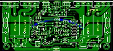
What is a PCB?
A Printed Circuit Board (PCB) is a flat board made of non-conductive material (such as fiberglass) with conductive copper traces that connect electronic components. PCBs eliminate the need for complex wiring and allow for more compact and efficient designs.
Key elements of a PCB
- Substrate: The base material that holds components.
- Copper Traces: Conductive pathways for electrical signals.
- Components: Resistors, capacitors, ICs, diodes, and more.
- Silkscreen Layer: Labels and component identifiers.
- Schematic Diagram: A blueprint that shows how components connect.
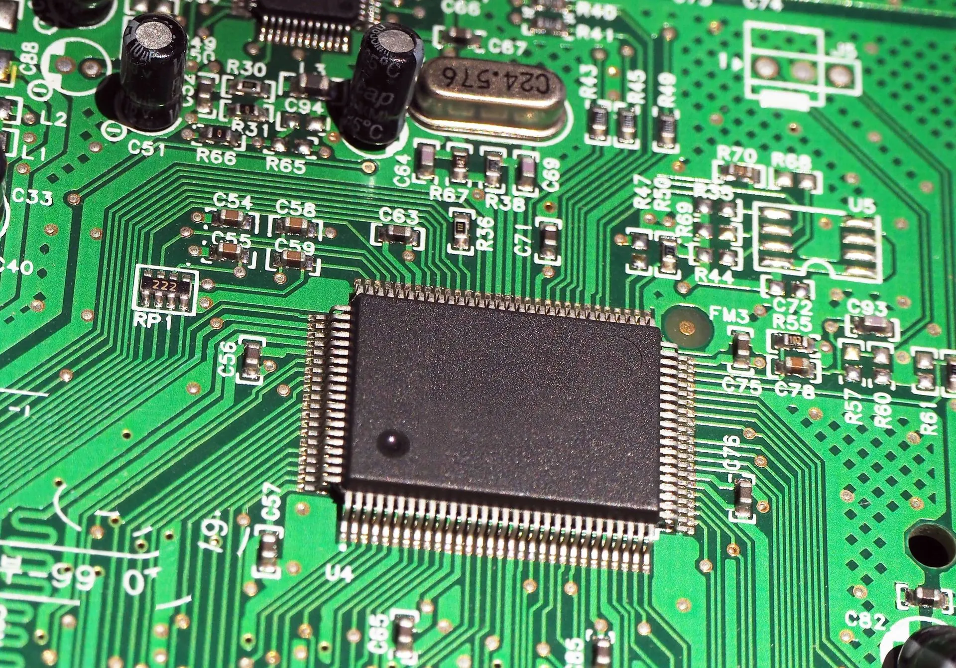
Identifying PCB Components
Understanding the components on a PCB is the first step in reading one. Here are the most common parts you’ll encounter:
Resistors
- Used to limit current and divide voltage.
- Identified by their rectangular shape and color-coded bands (or numerical values for SMD resistors).
Capacitors
- Store and release electrical energy.
- Can be ceramic (small, disc-shaped) or electrolytic (cylindrical, with polarity markings).
Inductors
- Store energy in a magnetic field.
- Appear as small coils or wire-wound components.
Diodes
- Allow current to flow in one direction only.
- Marked with a strip indicating the cathode (-).
Transistors
- Act as switches or amplifiers.
- Identified by three legs: collector, base, and emitter.
Integrated Circuits (ICs)
- Contain multiple electronic circuits in one package.
- Have a notch or dot indicating Pin 1.
Connectors & Terminals
- Used for power input, signal connections, and data transfer.
- Marked as J1, J2, P1, etc.
Switches & Buttons
- Used for user inputs.
- Found as tactile buttons, DIP switches, or rotary switches.
Understanding PCB Schematics & Symbols
A schematic diagram represents the electronic circuit of a PCB using symbols. Learning to interpret these symbols is crucial for reading a PCB.
Key Schematic Symbols
- Lines: Represent wires or electrical connections.
- Resistors (R): Zigzag lines.
- Capacitors (C): Parallel lines (polarized capacitors have a + sign).
- Diodes (D): Triangle pointing to a line.
- Transistors (Q): Three-terminal symbols.
- ICs (U): Rectangles with numbered pins.
Reading a Schematic Diagram
- Follow the Power Flow: Locate the power source (VCC, GND) and trace how power flows through components.
- Identify Input & Output: Understand how signals enter and exit the circuit.
- Use Reference Designators: Components are labeled as R1, C1, D1, etc.
- Check Connections & Traces: Ensure continuity and verify how each part connects.
Interpreting PCB Layout & Tracing Circuits
Once you understand the schematic, the next step is to interpret the actual PCB layout.
Layer Identification
PCBs can be single-layer, double-layer, or multi-layer:
- Single-layer: Components and traces on one side.
- Double-layer: Traces on both sides.
- Multi-layer: Internal copper layers for complex circuits.
Identifying PCB Traces & Pads
- Traces are the conductive pathways connecting components.
- Pads are small copper areas where component leads attach.
- Via Holes connect different PCB layers electrically.
How to Trace PCB Circuits
- Start from Power & Ground: Identify power (VCC) and ground (GND) traces.
- Follow the Signal Path: Use a multimeter in continuity mode to trace connections.
- Compare with the Schematic: Verify that PCB layout matches the schematic diagram.
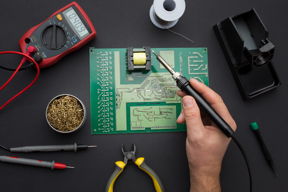
Troubleshooting PCBs
Reading a PCB is crucial when troubleshooting electronic devices. Here are key steps to diagnose and fix PCB issues:
Check for Visual Damage
- Burnt components, broken traces, and discoloration indicate failure.
- Use a magnifying glass or microscope for small components.
Use a Multimeter for Testing
- Continuity Test: Check if traces are intact.
- Voltage Test: Measure voltages at different points.
- Resistance Test: Verify resistor values.
Identify Faulty Components
- Overheated or swollen capacitors should be replaced.
- ICs with burnt marks indicate failure.
- Broken solder joints need re-soldering.
Compare a Working PCB
If available, use a working board for reference.
Best Practices for PCB Reading & Debugging
- Label Components: Use a PCB silkscreen for easy identification.
- Use Proper Tools: A digital multimeter, oscilloscope, and logic analyzer can help with troubleshooting.
- Refer to Manufacturer Datasheets: Get specifications for ICs and components.
- Practice on Simple PCBs: Start with basic circuits before moving to complex designs.
Advanced Topics in PCB Reading
As you advance, consider learning about:
- Surface Mount Technology (SMT) vs. Through-Hole Technology (THT)
- Multi-layer PCB Routing & Ground Planes
- High-Speed PCB Design & Signal Integrity
- Automated PCB Debugging Tools
Conclusion
Learning how to read a PCB is a fundamental skill for anyone in electronics. By understanding components, schematics, and layout interpretation, you can troubleshoot circuits, design your own boards, and work efficiently in the field of electronics.
By following this guide, beginners can build confidence in PCB reading, while professionals can refine their skills further. Keep practicing, use the right tools, and soon, reading a PCB will become second nature!