Printed Circuit Boards (PCBs) are the backbone of almost every electronic device we use today, from smartphones and computers to home appliances and industrial machinery. Making a PCB board may seem complex, but with the right tools and knowledge, it’s a process that can be mastered. In this guide, we will walk you through the steps involved in creating a PCB from start to finish, with detailed insights on the materials, techniques, and tips you need to know.
What is a PCB?
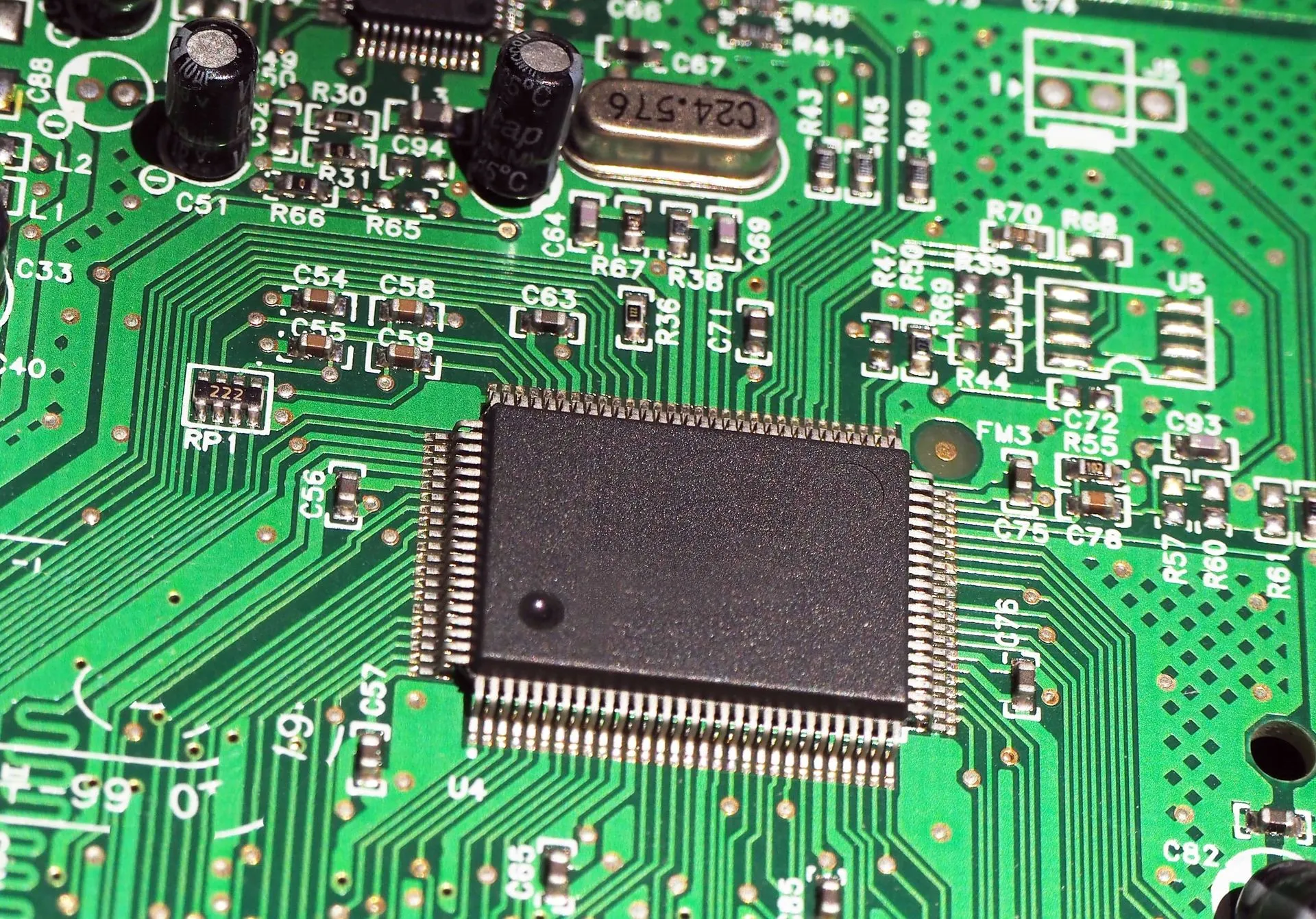
Before diving into the process, let’s quickly review what a PCB is. A PCB is a flat, rigid piece of material (typically fiberglass or epoxy) that connects and supports electronic components using conductive pathways, pads, and other features. It’s essential for allowing electrical signals to travel through a circuit, providing the foundation for virtually all modern electronics.
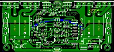
Design the PCB
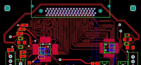
The first step in making a PCB is designing it. This involves creating a blueprint of the circuit that will be placed on the board. PCB design software, such as Eagle, KiCad, or Altium Designer, allows you to place components, draw traces, and design the layout of the circuit.
Key considerations when designing a PCB:
- Component Placement: Position the components on the board in a way that ensures efficient routing of traces and minimizes interference.
- Trace Width: Define the thickness of the copper traces based on the current they will carry.
- Via and Hole Placement: Decide on where vias (small holes for connecting layers of the PCB) and through-holes will be located.
- Design Rules Check (DRC): Run a design rules check to ensure that your layout adheres to the required standards, like trace width, clearance, and hole sizes.
Once you’ve designed the PCB, you’ll need to export it in a format that can be used for manufacturing, such as Gerber files.
Print the PCB Design
After your PCB design is finalized, you can move on to printing the design. This process involves transferring your PCB layout onto a physical board. There are two main methods for this:
- Laser Printer Method: Print the PCB design on glossy paper using a laser printer. Afterward, you can transfer the toner to a copper-clad board using heat.
- UV Exposure Method: For more precise results, the PCB design can be printed onto a transparent film and then exposed to UV light. The areas exposed to the light harden, and the rest can be washed away.
Prepare the Copper-Clad Board
A copper-clad board is the base material used for the Printed Circuit Boards. It typically consists of a non-conductive substrate (often fiberglass or phenolic) coated with a thin layer of copper on both sides.
- Cutting the Board: Start by cutting your copper-clad board to the desired dimensions using a saw or PCB board cutting tool.
- Cleaning: Use a fine abrasive pad or steel wool to clean the copper surface, removing any oxidation or dirt. This ensures that the toner or UV exposure process will transfer properly.
Etching the PCB
Etching is the process that removes unwanted copper from the board, leaving behind only the copper traces that form the electrical paths.
- Apply the Design: After transferring the design onto the copper board, use a chemical etching process to remove the unneeded copper. The most common etching solution is a mixture of ferric chloride and water.
- Etching Process: Place the copper-clad board into the etching solution. The areas not protected by the toner or resist material will be etched away, leaving the desired copper traces.
- Rinsing and Drying: Once etching is complete, rinse the board thoroughly with water to remove the etching solution. Allow the board to dry completely before proceeding.
Drilling Holes
Drilling holes is essential for inserting components into the PCB board. This can include both through-holes for components like resistors, capacitors, and connectors, as well as vias for inter-layer connections.
- Use a Drill Press: A precision drill press is recommended for drilling the holes. You’ll need to follow the drill pattern created during the PCB board design step.
- Drill Bit Size: Choose drill bits that match the hole sizes specified in your design. A typical size for most components is between 0.8mm and 1.2mm.
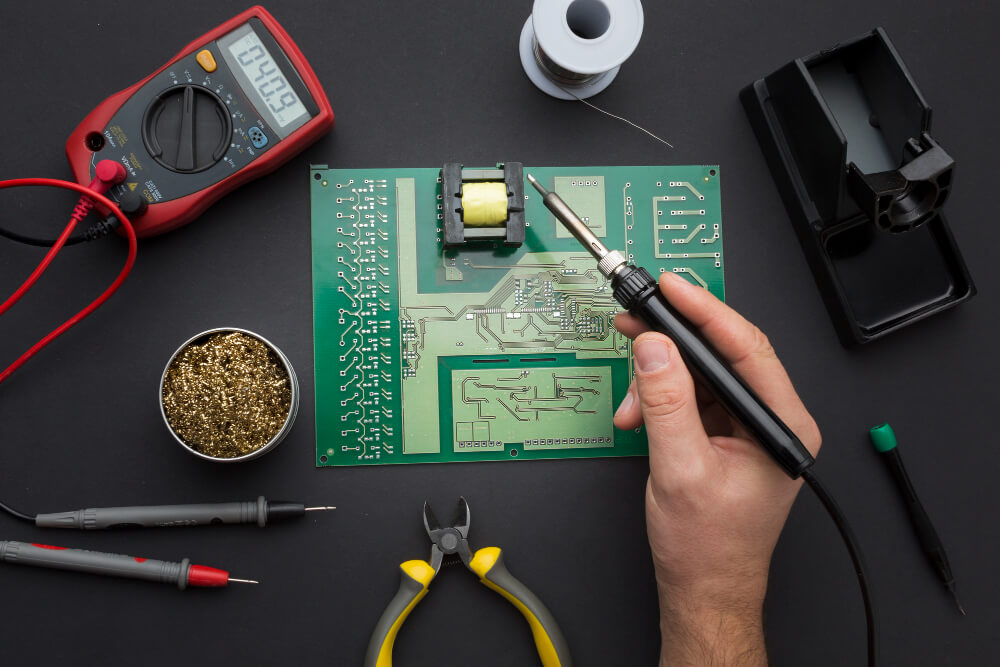
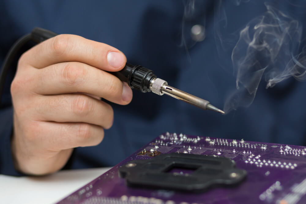
Soldering Components
Once the PCB is drilled, it’s time to place and solder the components onto the board. This step is critical, as poor soldering can lead to unreliable connections, causing circuit failure.
- Place Components: Insert the components through the drilled holes or position them on the surface (for surface-mount components).
- Soldering: Use a soldering iron and solder wire to make electrical connections. For surface-mount components, solder paste and a reflow oven can be used for efficient and precise soldering.
- Inspection: After soldering, inspect the board for any solder bridges (unintended connections between pads) and cold solder joints. A magnifying glass or microscope can help you spot small issues.
Testing the PCB Board
Once the components are soldered onto the PCB board, it’s time to test the circuit to ensure that everything works as intended. You can use a multimeter to check for continuity and verify that all connections are intact. It’s also a good idea to perform functional tests based on your circuit’s purpose.
Types of Tests:
- Continuity Test: Check that all traces and connections are correctly made.
- Voltage Test: Measure the voltage at various points in the circuit to ensure it operates correctly.
- Functional Test: Power up the circuit and observe its behavior in the real-world scenario.
Conclusion
Making a PCB board is a complex but rewarding process. By following these steps—designing the board, printing, etching, drilling, soldering, and testing—you can create your own custom PCBs for various electronics projects. While creating PCBs at home can be labor-intensive, it’s a great way to learn about electronics and circuit design. Whether you are building a small prototype or scaling up for larger production, mastering the art of PCB board creation opens up endless possibilities for innovation.