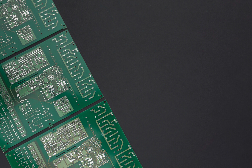
In the world of electronics, Printed Circuit Boards (PCBs) are the foundation upon which virtually all devices are built. Among the various types of PCBs available, Single-Layer PCBs stand out for their simplicity, reliability, and affordability. While they may seem basic compared to multi-layer or flexible boards, single-layer PCBs offer several hidden benefits that make them the go-to choice for a wide range of applications.
Whether you’re a startup looking for a cost-effective PCB solution, an engineer designing a simple device, or a manufacturer aiming to produce high-volume products, understanding the full potential of Single-Layer PCBs can help you make smarter decisions in electronics design and production.
What Are Single-Layer PCBs?
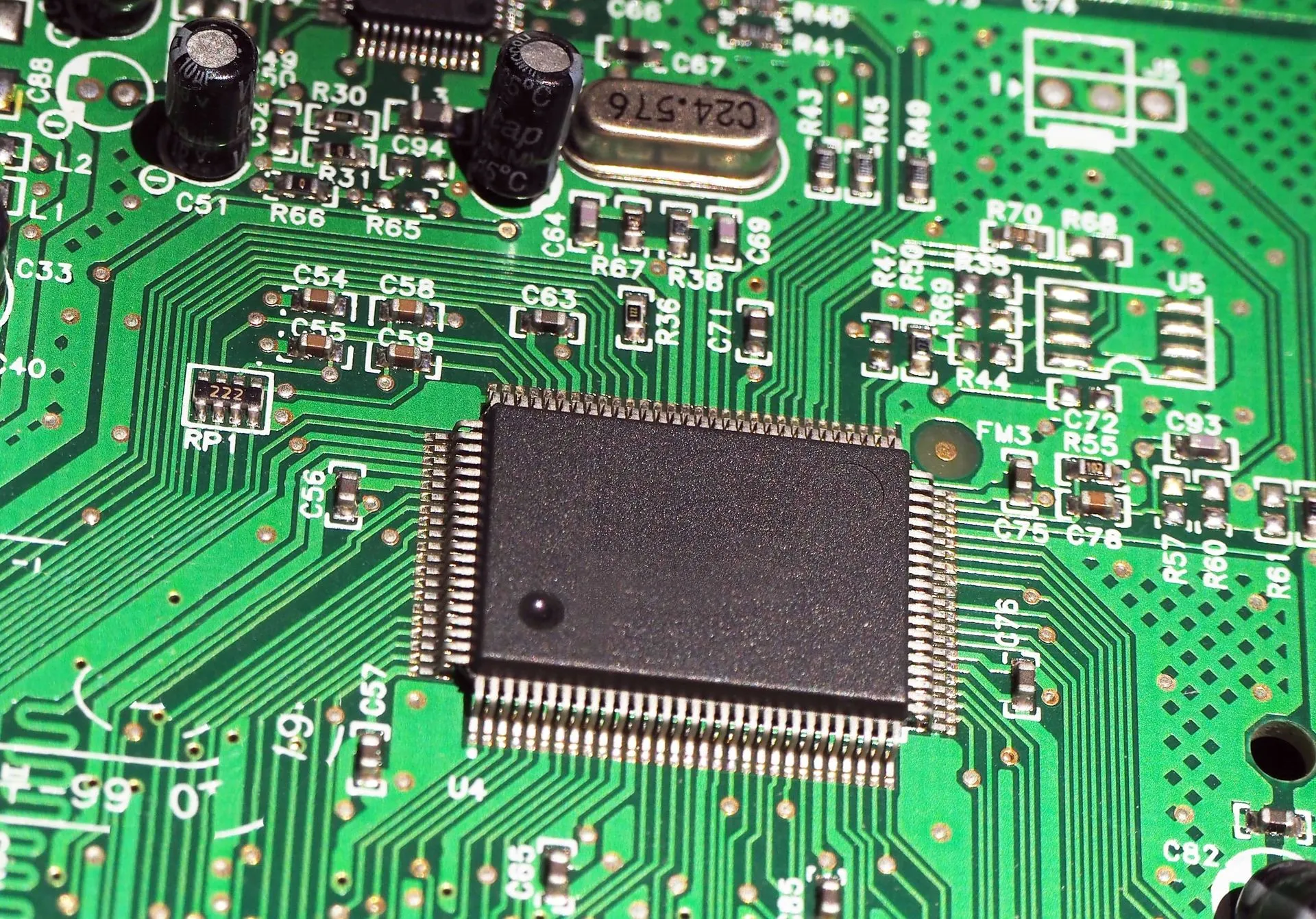
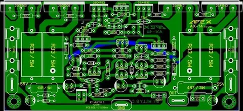
Single-Layer PCBs, also known as single-sided PCBs, are circuit boards that have conductive components and circuits on only one side. Typically made of a base substrate (such as FR4 or phenolic), a layer of conductive metal (usually copper) is applied to one side, and the other side is left blank. This straightforward design supports components like resistors, capacitors, and ICs on a single surface.
These basic circuit boards are ideal for low-density designs where routing complexity is minimal. Despite their apparent simplicity, they are indispensable in the electronics industry.
Hidden Benefits of Single-Layer PCBs
1. Affordability Without Sacrificing Functionality
One of the most significant advantages of Single-Layer PCBs is their low cost. Because the design and manufacturing processes are straightforward, they require fewer materials, tools, and production steps. This makes them an excellent choice for cost-effective PCB solutions, especially for products that do not require complex circuitry.
For small businesses or startups working with limited budgets, single-layer PCBs are a practical entry point into electronics development without cutting corners on quality.
2. Simplified PCB Design and Manufacturing
Single-layer PCBs are incredibly easy to design, especially when compared to multi-layer boards that involve intricate routing between different layers. Designers can use basic software to layout the circuit, and manufacturers can produce the boards with minimal turnaround time.
Because of this simplified PCB design, prototyping becomes faster and more efficient. If you’re iterating through multiple circuit concepts, single-layer PCBs are perfect for prototype circuit boards that can be tested and refined quickly.
3. High Reliability and Lower Risk of Failure
Fewer layers mean fewer potential points of failure. Multi-layer boards require through-hole plating and more complex interconnections, which increase the chance of manufacturing defects. On the other hand, Single-Layer PCBs are less prone to issues like short circuits, misalignments, or delamination.
Their durability and low error rate make them ideal for products requiring consistent performance over time, such as household appliances, basic lighting systems, and toys.
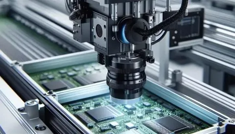
4. Faster Production Cycles
In a fast-paced market, speed matters. Single-layer PCBs can be produced in significantly less time than their multi-layer counterparts. Since they require fewer fabrication steps, manufacturers can fulfill large orders more rapidly.
This makes Single-Layer PCBs especially valuable in consumer electronics where demand fluctuations require manufacturers to scale production swiftly without compromising delivery schedules.
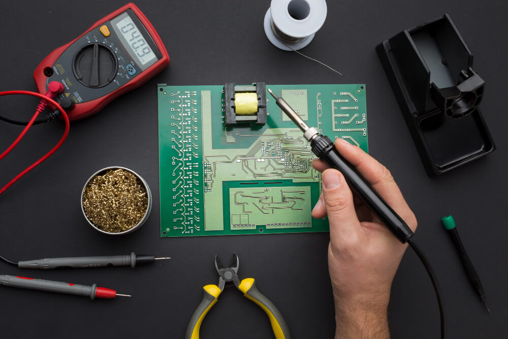
5. Easier Troubleshooting and Repairs
When issues arise in complex electronic systems, pinpointing the source can be a time-consuming process. Single-layer PCBs simplify this by allowing technicians to visually inspect and test all components from one side. This transparency makes debugging, repairing, and modifying circuits a breeze.
For repair centers or DIY enthusiasts, the accessibility of these boards offers significant long-term benefits.
6. Energy Efficiency and Thermal Management
Because these boards have just one conductive layer, there’s less heat buildup compared to densely packed multi-layer PCBs. This contributes to better thermal management, especially in low-power applications. While they might not be suitable for high-frequency or high-current uses, they’re ideal for low-energy devices.
Applications such as LED lighting, calculators, and simple sensor systems benefit from this energy-efficient design.
Common Applications of Single-Layer PCBs
Due to their low cost and simplicity, Single-Layer PCBs are widely used across industries. Some typical applications include:
- Consumer electronics: Radios, remotes, digital clocks
- LED lighting systems: Simple driver circuits for LEDs
- Power supplies: Chargers, battery packs
- Automotive electronics: Basic dashboard components and sensors
- Industrial equipment: Control panels and indicators
- Educational kits: Basic training boards and electronic learning kits
In each of these scenarios, the need for a high-performance, cost-effective PCB with minimal complexity makes single-layer boards the logical choice.
Environmental Impact and Sustainability
With increasing awareness of sustainability in electronics manufacturing, single-layer PCBs are also gaining recognition for their relatively low environmental footprint. They consume fewer raw materials, use less energy in production, and are easier to recycle due to their simplified structure.
By choosing Single-Layer PCBs for suitable applications, manufacturers contribute to greener production processes, aligning with eco-conscious business goals.
Single-Layer vs. Multi-Layer: When to Choose Simplicity
While multi-layer PCBs are necessary for high-performance devices like smartphones, computers, and telecommunications equipment, they are often overkill for simpler products. Opting for Single-Layer PCBs when appropriate can result in significant cost and time savings.
Here’s a quick comparison:
| Feature | Single-Layer PCBs | Multi-Layer PCBs |
|---|---|---|
| Complexity | Simple | High |
| Cost | Low | High |
| Design Time | Short | Long |
| Manufacturing Process | Easy | Complex |
| Ideal for | Basic electronics, prototyping | Advanced systems, compact design |
Understanding the needs of your project is key to making the right decision. In many instances, choosing a single-layer option can streamline development without compromising on essential functionality.
Future-Proofing with Simplicity
As the Internet of Things (IoT) and smart devices continue to grow, many new applications are emerging that do not require high-performance processing. Smart tags, wearable accessories, and micro-sensors can all be powered using Single-Layer PCBs, allowing designers to keep products compact, efficient, and affordable.
This trend indicates that, despite being one of the oldest types of PCBs, the relevance of single-layer designs is far from diminishing.
Final Thoughts
While multi-layer PCBs often steal the spotlight with their complexity and performance, Single-Layer PCBs quietly power a large portion of everyday electronics. Their hidden benefits — cost-efficiency, simplicity, speed, and reliability — make them an essential part of modern electronics manufacturing.
At Qual-Pro, we recognize the value and versatility that single-layer designs bring to a wide range of industries. Whether you’re launching a new product, building prototypes, or producing high-volume electronics, Single-Layer PCBs offer a smart, scalable, and dependable solution.
If you’re looking to minimize costs, simplify your design process, and ensure consistent performance, trust Qual-Pro to deliver PCB solutions that meet your exact needs — because sometimes, the simplest solution is the most powerful.