In the world of electronics manufacturing, ensuring the reliability and functionality of printed circuit boards (PCBs) is paramount. Quality control methods play a crucial role in identifying and rectifying defects during the assembly process, thereby guaranteeing the performance and longevity of electronic devices.
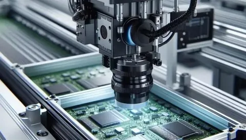
Automated Optical Inspection (AOI)
Automated Optical Inspection (AOI) employs high-resolution cameras and advanced image processing software to inspect PCBs for defects such as misalignment, solder bridges, and missing components. This non-contact method is widely utilized due to its speed and accuracy.
Benefits:
- High Throughput: AOI systems can inspect large volumes of PCBs rapidly, making them ideal for high-speed production lines.
- Early Detection: By identifying defects early in the assembly process, AOI helps in minimizing costly rework and ensuring product quality.
- Consistency: Automated systems provide consistent inspection results, reducing the variability associated with manual inspections.
Limitations:
- Surface-Level Detection: AOI primarily detects surface defects and may not identify issues beneath components, such as solder joint integrity.
- Dependence on Lighting Conditions: The effectiveness of AOI can be influenced by lighting conditions and the quality of the camera system
In-Circuit Testing (ICT)
In-Circuit Testing (ICT) involves using test probes to check the electrical performance of individual components on a populated PCB. This method can identify issues like short circuits, open circuits, and incorrect component values.
Benefits:
- Comprehensive Testing: ICT provides a thorough assessment of each component’s functionality, ensuring that the assembled PCB operates as intended.
- Early Fault Detection: By identifying faults early, ICT helps in reducing the risk of field failures and enhancing product reliability.
- Cost-Effective: Detecting and rectifying faults during the assembly process is more cost-effective than addressing issues post-production.
Limitations:
- High Initial Setup Cost: The setup for ICT requires specialized fixtures and equipment, which can be costly.
- Limited to Accessible Components: ICT may not be effective for testing components that are not easily accessible or are hidden beneath other parts.
Solder Paste Inspection (SPI)
Solder Paste Inspection (SPI) is conducted before component placement in the PCB assembly process. This automated inspection method uses advanced optical systems to verify the quality and quantity of solder paste deposited on the PCB pads and checks for solderability.
Benefits:
- Prevention of Soldering Defects: SPI helps in identifying issues like insufficient solder paste or bridging before component placement, preventing soldering defects.
- Enhanced Solder Joint Quality: By ensuring optimal solder paste application, SPI contributes to the formation of reliable solder joints.
- Improved Yield: Early detection of solder paste issues leads to higher first-pass yields and reduced rework.
Limitations:
- Requires Calibration: SPI systems need regular calibration to maintain accuracy and reliability.
- Dependency on Paste Characteristics: The effectiveness of SPI can be influenced by the characteristics of the solder paste used.

Functional Testing
Functional Testing involves verifying that the assembled PCB performs its intended function under simulated operating conditions. This method ensures that the PCB operates as expected in its final application.
Benefits:
- Real-World Simulation: Functional testing simulates actual operating conditions, providing a realistic assessment of the PCB’s performance.
- Detection of Complex Issues: This method can uncover issues that may not be apparent through other testing methods, such as intermittent faults or performance degradation over time.
- Assurance of Product Quality: By confirming that the PCB meets its functional specifications, functional testing ensures the delivery of high-quality products to customers.
Limitations:
- Time-Consuming: Functional testing can be time-consuming, especially for complex PCBs with numerous functions.
- Resource Intensive: Setting up and conducting functional tests requires specialized equipment and resources.
Automated X-Ray Inspection (AXI)
Overview:
Automated X-Ray Inspection (AXI) uses X-ray imaging to inspect the internal structures of a PCB, such as solder joints beneath components. This method is particularly useful for detecting hidden defects that are not visible through other inspection methods.
Benefits:
- Internal Defect Detection: AXI can identify issues like voids, cracks, and insufficient solder beneath components, which are critical for the reliability of the PCB.
- Non-Destructive Testing: Being a non-destructive method, AXI allows for thorough inspection without damaging the PCB.
- High Accuracy: AXI provides high-resolution images, enabling precise detection of internal defects.
Limitations:
- High Cost: AXI equipment is expensive, making it more suitable for high-volume production runs.
- Complex Interpretation: Interpreting X-ray images requires skilled personnel and can be complex.
Conclusion
Implementing robust quality control methods is essential for ensuring the reliability and performance of PCBs in electronic devices. Each of the methods discussed—Automated Optical Inspection (AOI), In-Circuit Testing (ICT), Solder Paste Inspection (SPI), Functional Testing, and Automated X-Ray Inspection (AXI)—offers unique advantages and plays a pivotal role in the PCB assembly process.
At Qual-Pro, we are committed to delivering high-quality PCB assemblies by employing these advanced quality control methods. Our rigorous quality assurance processes ensure that every PCB meets the highest standards of performance and reliability.