In the fast-paced world of electronics development, having the right PCB Design Software can make or break your project. From hobbyists creating DIY gadgets to engineers working on complex industrial systems, PCB design tools have become an essential part of modern electronics. But with the rapid evolution of technology, the landscape of PCB Design Software in 2025 has shifted dramatically.
So, what’s the best PCB software for your needs this year? Let’s dive into the latest innovations, key players, and essential features you should look for to create smarter, faster, and more reliable printed circuit boards.
What Is PCB Design Software?
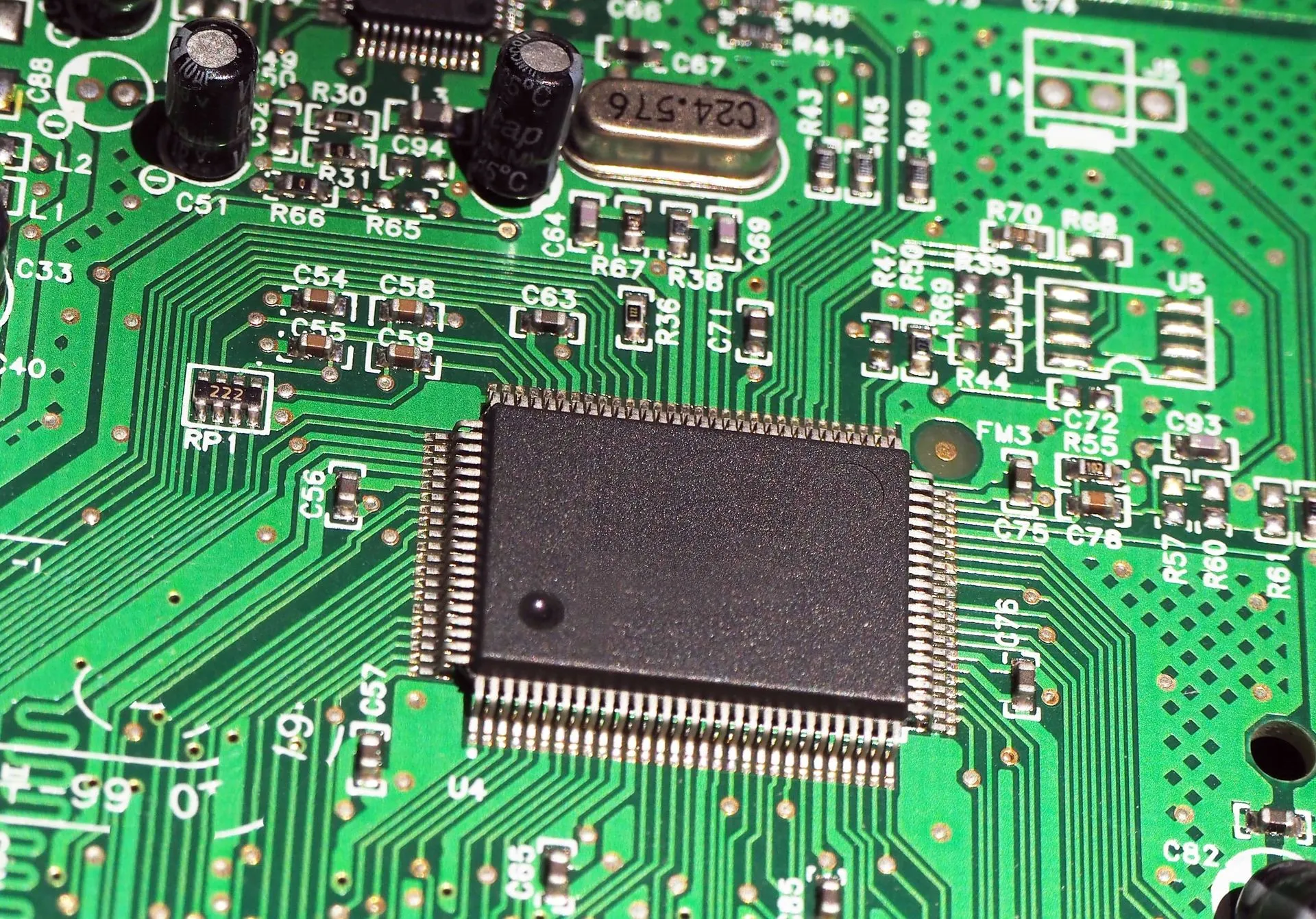
PCB Design Software is a specialized set of tools used to design the layout, electrical connections, and mechanical configuration of a printed circuit board (PCB). It allows designers to convert electronic schematics into a visual and physical layout that can be manufactured and assembled into real-world products.
Typical software includes features for schematic capture, PCB layout, design rule checking (DRC), 3D modeling, and sometimes circuit simulation tools. These features are essential for ensuring that a circuit functions as intended and can be efficiently produced.
Why PCB Design Software Matters in 2025
In 2025, the demand for more compact, powerful, and reliable electronic devices continues to grow. With technologies like IoT, AI, wearables, and electric vehicles booming, designers need advanced tools to meet new challenges.
Modern PCB Design Software now integrates AI-assisted routing, cloud-based collaboration, real-time simulation, and even manufacturing previews. Choosing the right software isn’t just about functionality—it’s about productivity, speed, and accuracy.
Top PCB Design Software in 2025
1. Altium Designer 2025
Still considered the gold standard in PCB Design Software, Altium Designer continues to lead the pack in 2025. Known for its user-friendly interface, robust schematic capture tools, and real-time component libraries, Altium now offers:
- AI-powered routing suggestions
- Built-in cloud storage and team collaboration
- Integrated simulation and signal integrity analysis
- Enhanced 3D visualization for mechanical fit checks
Its all-in-one nature makes it ideal for both small startups and enterprise-level design teams.
2. KiCad 7
For open-source enthusiasts, KiCad remains one of the most powerful free options. Version 7, released in late 2024, brought major improvements that made it a contender even for professional projects. Key features include:
- Real-time 3D rendering of boards
- Accurate DRC (Design Rule Checks)
- Extensive library management tools
- Improved circuit simulation tools using ngspice
As a free solution with no licensing costs, KiCad is perfect for students, hobbyists, and budget-conscious developers.
3. Autodesk Fusion 360 with Eagle
Fusion 360’s integration with Eagle PCB design makes it a versatile choice for users needing both mechanical and electronic design in one package. In 2025, Autodesk continues to streamline the experience with:
- Cloud-based team collaboration
- Real-time component syncing
- Seamless transition from circuit board design to mechanical CAD
- Embedded manufacturing previews
It’s particularly strong in industries like robotics, drones, and industrial automation where tight mechanical integration is crucial.
4. OrCAD and Allegro by Cadence
For large-scale and high-frequency applications, OrCAD and Allegro remain industry favorites. In 2025, they continue to lead in areas like:
- High-speed design for 5G and automotive
- Thermal and signal integrity analysis
- Multiboard system integration
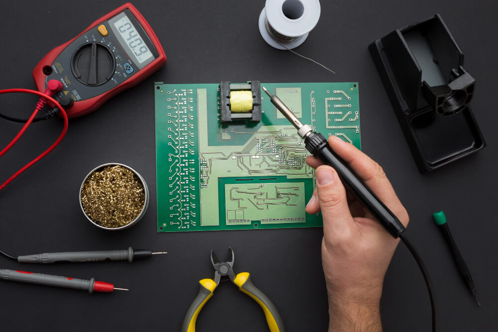
- Advanced PCB prototyping capabilities
While not beginner-friendly, these tools are indispensable for advanced electronic design automation (EDA) professionals.
5. EasyEDA Pro
Ideal for beginners and rapid prototyping, EasyEDA Pro offers an easy-to-use online platform with integrated PCB manufacturing through JLCPCB. Notable 2025 updates include:
- Smart auto-routing
- Online component sourcing integration
- Simulation support for analog/digital circuits
- One-click PCB order and fabrication
If you’re a maker or startup developing MVPs, EasyEDA can take you from idea to production within days.
Key Features to Look for in 2025 PCB Design Software
Choosing the right PCB Design Software depends on your project’s complexity, budget, and workflow. Here are the must-have features to look for:
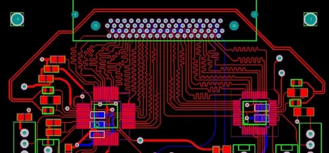
1. Schematic Capture and Netlist Generation
Schematic capture is the first step in any circuit board design process. The software should allow you to easily place components, assign net connections, and automatically generate a netlist for PCB layout.
2. Advanced Routing Capabilities
Modern boards require precision routing. Look for tools offering AI-assisted routing, differential pair management, and autorouting for complex paths.
3. 3D Visualization and Mechanical Integration
In 2025, many PCB layout tools come with built-in 3D views, helping designers visualize component placement and check for mechanical interferences.

4. Design Rule Checks (DRC)
DRC engines help prevent costly errors by flagging rule violations during the layout process. Make sure your software supports customizable DRC profiles.
5. Simulation and Analysis Tools
Some PCB Design Software includes circuit simulation tools to validate performance before prototyping. This saves time and reduces the need for multiple revisions.
6. Library and BOM Management
Component libraries and automated Bill of Materials (BOM) generation streamline the procurement process. Integration with supply chain databases is a plus.
7. Cloud-Based Collaboration
As remote work becomes more common, real-time team collaboration tools and cloud storage are essential for design continuity.
Benefits of Modern PCB Design Software
The evolution of PCB Design Software isn’t just about flashy features—it’s about real-world benefits:
- Speed: Faster prototyping, routing, and manufacturing preparation
- Accuracy: Automated checks and simulations reduce human error
- Scalability: Handle projects from simple hobby boards to multi-layer industrial systems
- Integration: Seamless flow from schematic to layout to fabrication
- Collaboration: Teams can now work in real time from anywhere in the world
These benefits are driving a new wave of electronics innovation, making 2025 an exciting time for PCB developers.
PCB Design Trends in 2025
Several key trends are influencing PCB Design Software development this year:
- AI-Powered Design Assistants: Helping with component placement, routing, and optimization
- Cloud-First Platforms: Reducing reliance on local installations and improving accessibility
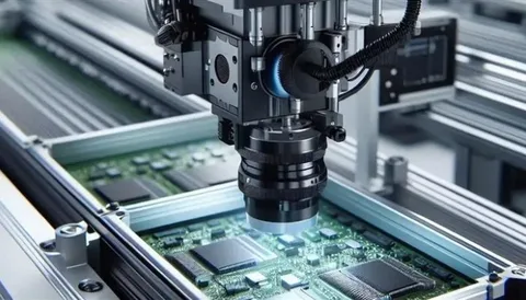
- Integrated Fabrication Tools: Many tools now offer direct PCB ordering and DFM (Design for Manufacturing) checks
- Sustainable Design: Eco-friendly material selection and energy-efficient layouts are becoming more important
- Security Features: As more devices connect to the internet, secure hardware design is gaining attention
Staying ahead in PCB design means adopting tools that keep pace with these innovations.
Final Thoughts
In 2025, the world of PCB Design Software is smarter, faster, and more integrated than ever before. From open-source platforms like KiCad to professional-grade suites like Altium and OrCAD, designers have more options than ever to bring their circuits to life.
Whether you’re designing a high-speed communication device or building your first Arduino shield, choosing the right PCB Design Software can dramatically impact your productivity and final product quality.
At Qual-Pro, we understand how critical the right tools are in achieving design excellence. That’s why we stay ahead of the curve, leveraging the best PCB Design Software available to deliver precision-engineered solutions for every project. From concept to prototype to production—we help bring your vision to life with accuracy and speed.