In today’s fast-paced tech world, printed circuit boards (PCBs) form the invisible backbone of almost every electronic device. While single-layer PCBs offer simplicity and affordability, they can fall short in more complex designs. Enter the Double-Layer PCBs—a smart evolution in the PCB family that balances performance and affordability without diving into the complexities and high costs of multi-layer boards.
With two layers of conductive copper traces, Double-Layer PCBs provide the perfect foundation for moderately complex circuits that require a step up from single-sided boards. But what exactly makes them “smart”? Let’s explore the unique features, benefits, applications, and why they’ve become a cornerstone in modern electronics manufacturing.
What Are Double-Layer PCBs?
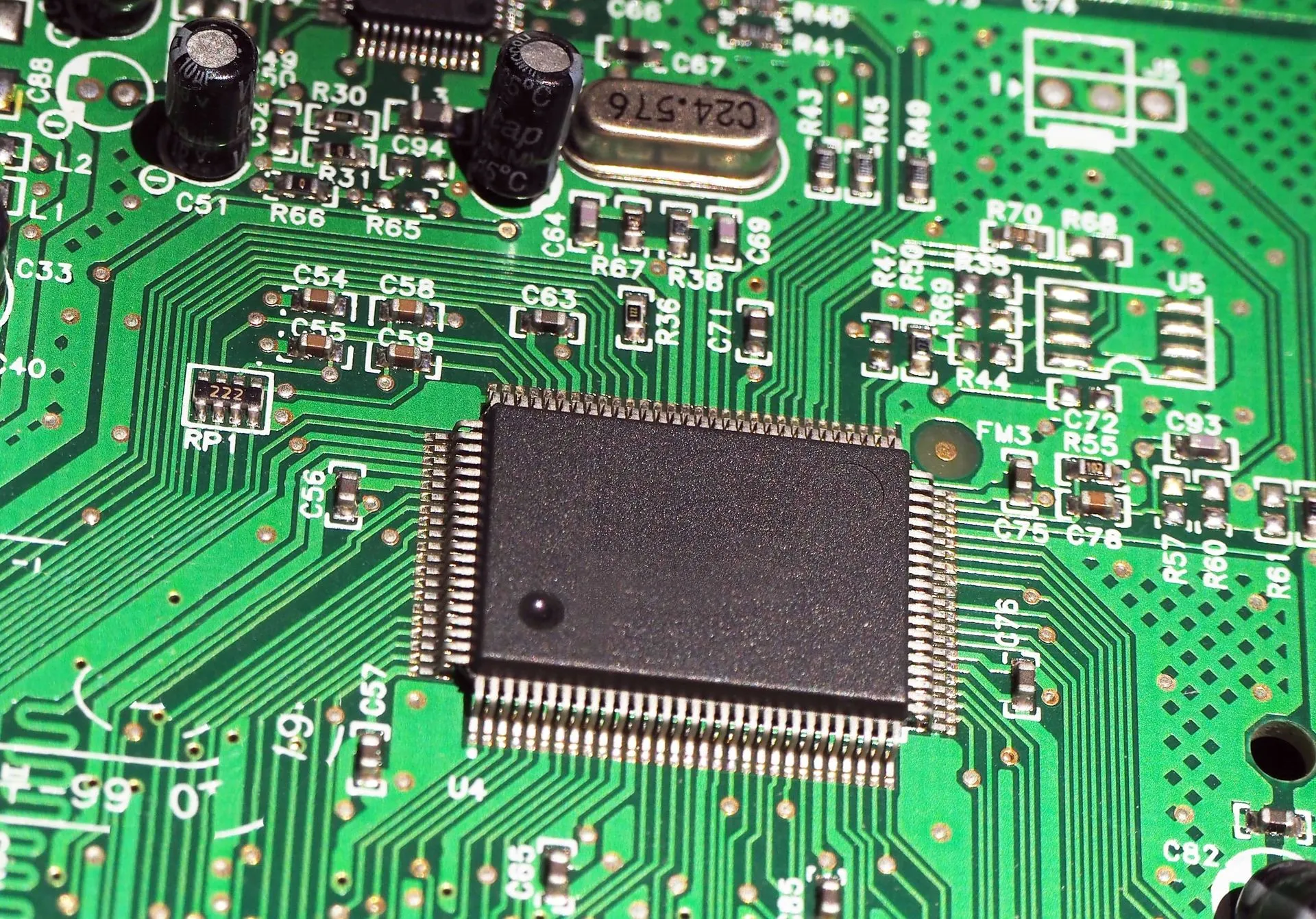
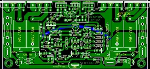
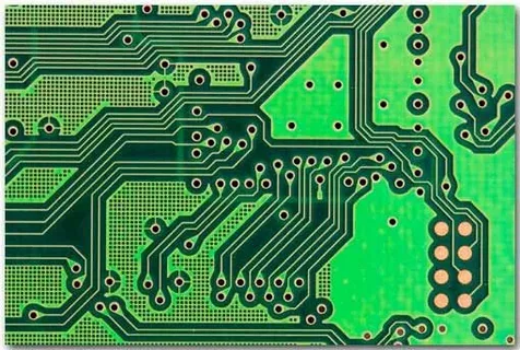
Double-Layer PCBs, also known as double-sided PCBs, have conductive copper layers on both the top and bottom of the board. Unlike single-layer boards, these PCBs allow for routing of circuits on both sides, often connected by vias—small holes drilled through the board and plated with conductive material. This design enables more intricate and compact circuitry.
These PCBs are often made using FR4, a fiberglass-reinforced epoxy laminate, but other materials like polyimide and aluminum are used depending on the application. The ability to route traces on both sides provides a significant improvement in circuit complexity and functionality.
Key Advantages of Double-Layer PCBs
1. Greater Design Flexibility
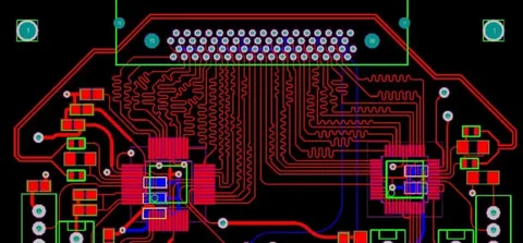
One of the primary reasons Double-Layer PCBs are considered a smart solution is the design flexibility they offer. With routing available on both sides, engineers can create more intricate designs without the need to jump to expensive multi-layer PCBs. This is particularly beneficial when working with complex circuits or needing to connect more electronic components.
Designers can reduce the size of the board, allowing more compact electronics and minimizing unnecessary layers or wasted space.
2. Improved Circuit Density
With access to both sides of the board, Double-Layer PCBs can host a higher density of components. This enables the creation of more powerful devices without increasing board size. It also helps reduce signal interference since ground and power planes can be better distributed, enhancing performance in many applications.
This characteristic makes them ideal for medium-complexity circuit boards where single-layer PCBs fall short but multi-layer PCBs aren’t necessary.
3. Enhanced Connectivity Through Vias
Through-hole technology and plated vias allow easy connectivity between the two layers. Vias act as bridges that connect traces from the top to the bottom, enabling smoother and more reliable signal paths. This improves electrical performance and offers greater routing possibilities in constrained layouts.
The use of vias in Double-Layer PCBs makes them well-suited for mixed-signal applications, where both analog and digital components need to coexist.
4. Cost-Effective Compared to Multi-Layer Boards
While more complex than single-sided PCBs, Double-Layer PCBs are still significantly more affordable than multi-layer PCBs. The additional complexity does raise production costs slightly, but the improvement in functionality justifies the investment for most mid-range applications.
This cost-performance ratio makes them popular in industries where moderate complexity and reliability are required without going over budget.
Common Applications of Double-Layer PCBs
Thanks to their balance between functionality and affordability, Double-Layer PCBs are used in a wide variety of sectors:
- Consumer Electronics: Audio systems, televisions, cameras, and gaming consoles
- Industrial Controls: Automation systems, HVAC controls, and industrial sensors
- Power Supplies: Switch-mode power supplies and inverters
- LED Systems: Complex lighting systems that require multiple controls or dimming options
- Automotive: Dashboards, engine management units, and infotainment systems
- Medical Devices: Diagnostic instruments and patient monitoring systems
In each of these domains, Double-Layer PCBs allow for compact, efficient circuit design while ensuring performance and reliability.
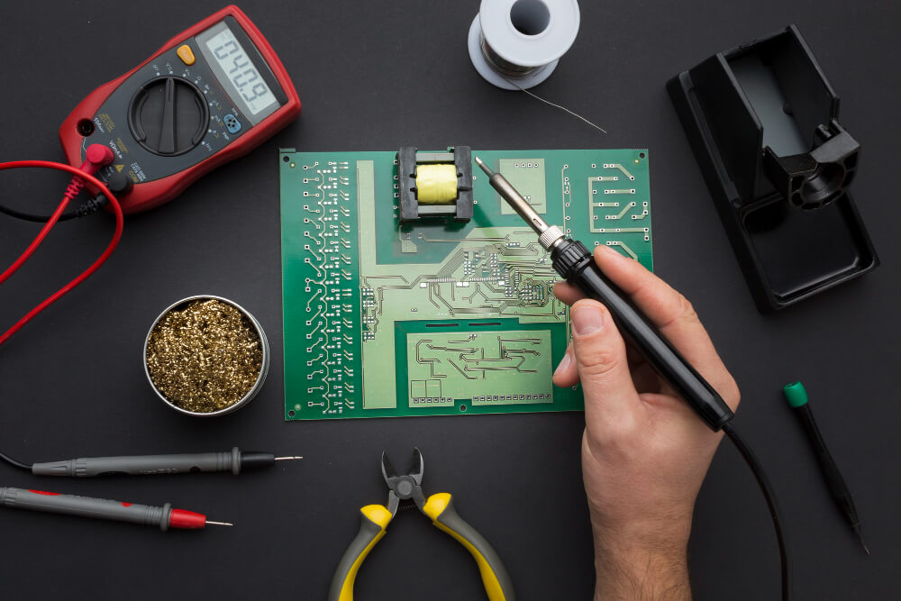
Manufacturing Process of Double-Layer PCBs
The fabrication of Double-Layer PCBs involves several steps:
- Base Material Preparation: A fiberglass or polymer base is laminated with copper on both sides.
- Drilling Vias: Holes are drilled where electrical connections are required between the top and bottom layers.
- Plating the Vias: The holes are plated with copper to ensure conductivity.
- Photoresist Application: A light-sensitive layer is applied to the board and then exposed to UV light through a mask containing the desired PCB layout.
- Etching: The board is etched to remove unwanted copper, leaving behind the desired circuitry.
- Solder Mask and Silkscreen: A protective solder mask is applied, followed by component labeling via silkscreen printing.
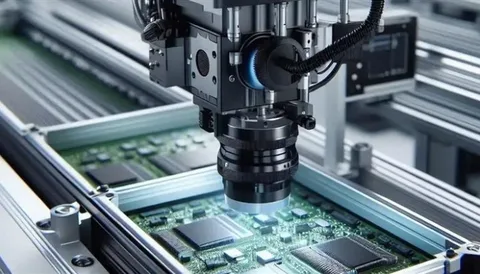
- Final Inspection and Testing: Electrical tests ensure that the PCB design is functioning correctly and meets all specifications.
Though more complex than single-layer boards, this process remains streamlined and cost-effective compared to multi-layer manufacturing.
Why Double-Layer PCBs Are a Smart Middle Ground
Choosing the right PCB depends on your project’s complexity, size, and budget. Double-Layer PCBs hit a sweet spot by offering:
- Increased functionality over single-layer PCBs
- A more compact footprint
- Lower cost compared to multi-layer PCBs
- Better thermal and signal performance
- Support for both surface-mount and through-hole components
For many applications, they offer the best of both worlds—enough complexity to support intricate designs without the high cost and manufacturing challenges of multi-layer PCBs.
Comparing PCB Types: A Quick Overview
| Feature | Single-Layer PCBs | Double-Layer PCBs | Multi-Layer PCBs |
|---|---|---|---|
| Layers | 1 | 2 | 3+ |
| Design Complexity | Low | Medium | High |
| Cost | Low | Moderate | High |
| Circuit Density | Limited | Moderate | High |
| Manufacturing Time | Short | Moderate | Long |
| Ideal Use Case | Basic electronics | Consumer/industrial | High-speed systems |
This table illustrates how Double-Layer PCBs provide a logical next step from basic designs while avoiding the costs associated with complex multi-layer configurations.
Future Trends and Smart Device Integration
As IoT (Internet of Things) and AI-integrated devices become more mainstream, the demand for smart, compact, and reliable PCBs is growing. Many smart devices, wearables, and industrial IoT modules find their needs met with Double-Layer PCBs, especially in early stages of development.
They also play a key role in rapid prototyping and small-batch production where speed, adaptability, and cost control are crucial. Their wide application potential ensures they will remain relevant for years to come.
Final Thoughts
In a world where electronics are evolving rapidly, Double-Layer PCBs provide a smart, efficient, and balanced solution for a wide array of applications. Their dual-sided design enables greater circuit density, better performance, and improved connectivity—all without the high costs and complexities of multi-layer alternatives.
For businesses, engineers, and manufacturers seeking reliability and flexibility, Double-Layer PCBs are an ideal middle ground. They offer the perfect combination of affordability and sophistication needed for modern electronic designs.
At Qual-Pro, we specialize in delivering high-quality, precision-engineered PCBs tailored to your needs. Whether you’re developing a new consumer product, prototyping an industrial solution, or optimizing an existing design, our Double-Layer PCB solutions are engineered to perform.
Ready to make a smarter choice in PCB design? Partner with Qual-Pro—where innovation meets reliability.