Designing a printed circuit board (PCB) layout is a crucial step in turning your electronic schematic into a physical, manufacturable board. The right PCB layout ensures reliability, efficiency, and performance of your electronic device. In this comprehensive guide, you will learn how to design a PCB layout in Qual-Pro Designer, a powerful tool favored by engineers for its intuitive interface and robust features.
Whether you are a beginner or have some experience, this article covers everything you need to create a professional PCB layout that meets your project requirements.
What is PCB Layout Design?
Before diving into the practical steps, it’s essential to understand what it means to design a PCB layout. This process involves arranging components, routing electrical connections, defining board layers, and preparing the design for manufacturing.
The PCB layout translates your circuit schematic into a blueprint that manufacturers use to produce the physical board. It’s not just about connecting components but optimizing space, minimizing interference, and ensuring signal integrity.
Why Use Qual-Pro Designer for PCB Layout?
Qual-Pro Designer stands out in the PCB design world for several reasons:
- User-Friendly Interface: Makes it easy for beginners and professionals alike.
- Advanced Routing Tools: Efficiently manage complex traces.
- Real-Time Error Checking: Helps avoid common design mistakes.
- Comprehensive Library: Access to a vast range of components.
- Seamless Schematic Integration: Works smoothly from schematic capture to layout.
With Qual-Pro Designer, you can confidently design a PCB layout that meets high-quality standards.
Design a PCB Layout Step-by-Step Guide
Prepare Your Schematic
The first step in any PCB project is to finalize your schematic. Ensure all components are correctly placed and connected in your circuit diagram. Qual-Pro Designer offers a schematic capture tool where you can:
- Add components from the library
- Define nets and connections
- Validate the schematic for errors
A clean and error-free schematic is critical because it serves as the foundation for your PCB layout.
Define Board Parameters
Once your schematic is ready, switch to the PCB layout workspace. Here, you need to set your board parameters:
- Board Shape and Size: Define the physical dimensions based on your project needs.
- Layer Stack-Up: Choose single-layer, double-layer, or multilayer options depending on circuit complexity.
- Design Rules: Set constraints for trace width, spacing, via sizes, and more to comply with manufacturing standards.
Defining these parameters early helps avoid costly revisions later.
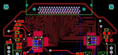
Place Components Strategically
Component placement is a critical phase in the design a PCB layout process. How you position components affects signal quality, thermal management, and ease of assembly.
In Qual-Pro Designer:
- Use the auto-placement tool for an initial layout.
- Manually adjust components for optimal placement.
- Group related components together to minimize trace lengths.
- Keep power and ground components accessible for better connectivity.
Good component placement reduces the complexity of routing and improves the overall board performance.
Route the PCB Traces
Routing is the process of creating electrical connections between components through copper traces. Qual-Pro Designer offers several routing options:
- Manual Routing: Provides full control over trace paths.
- Auto-Routing: Useful for complex designs but may require manual refinement.
- Interactive Routing: Combines both methods, allowing you to guide trace paths.
When routing, pay attention to:
- Signal Integrity: Avoid sharp angles and long trace lengths to reduce interference.
- Power Distribution: Use wider traces or planes for power lines.
- Ground Plane: Implement a continuous ground plane to minimize noise.
Remember, well-routed PCBs are easier to manufacture and yield better electrical performance.
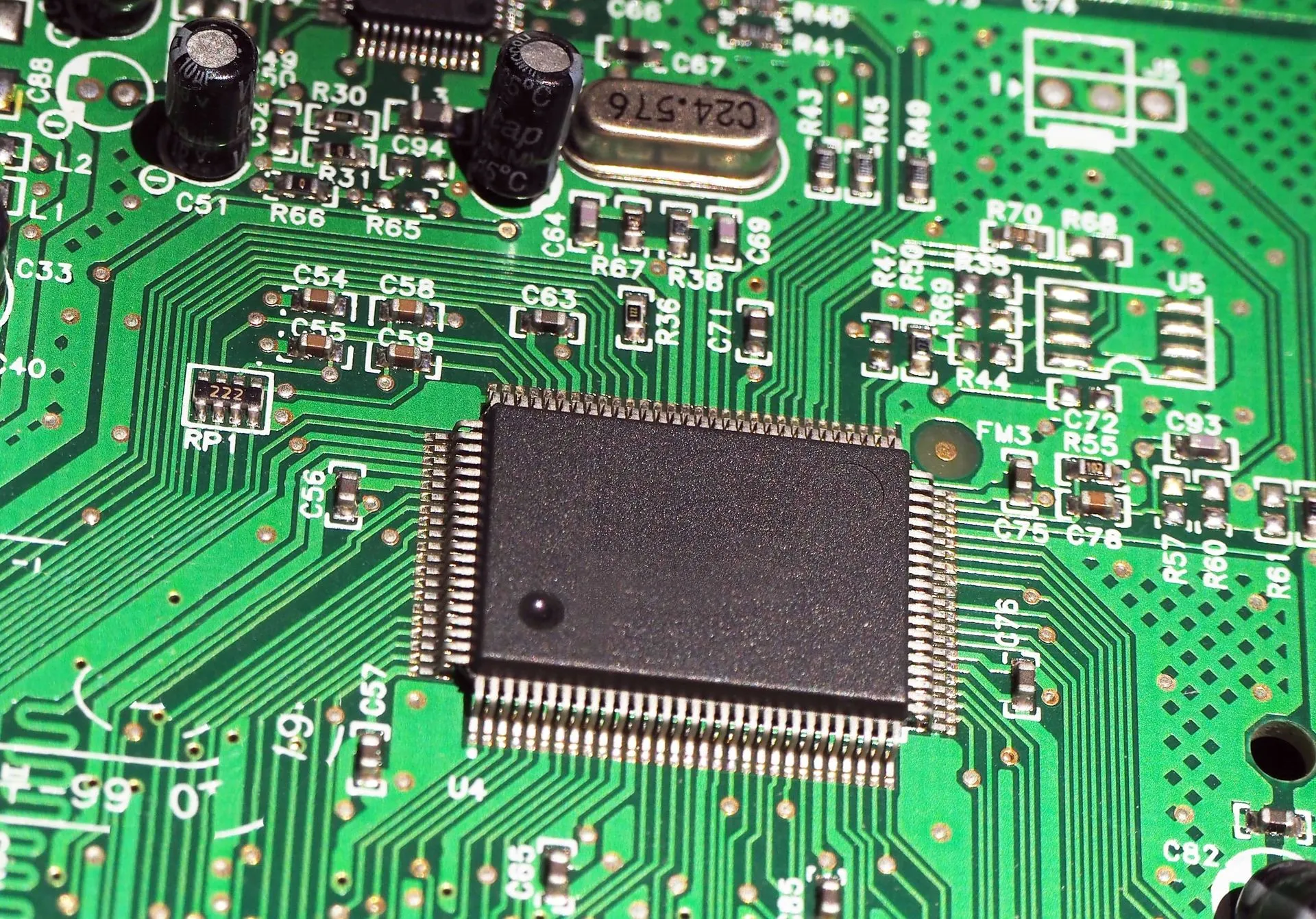
Add Vias and Pads
Vias are small conductive holes that connect traces between different layers of the PCB. Pads are the areas where components’ pins are soldered.
In your layout:
- Place vias carefully to maintain signal quality.
- Use the appropriate size for vias and pads based on component datasheets.
- Avoid placing vias too close to pads or traces to prevent shorts.
Qual-Pro Designer allows you to customize via and pad sizes, helping you meet both design and manufacturing requirements.
Run Design Rule Checks (DRC)
Before finalizing your PCB layout, run a Design Rule Check in Qual-Pro Designer. This automated check verifies that your layout meets all the predefined constraints such as:
- Trace widths and spacing
- Clearance between components and copper areas
- Drill hole sizes
- Electrical connectivity
Fixing errors flagged by the DRC early saves time and money by preventing manufacturing issues.
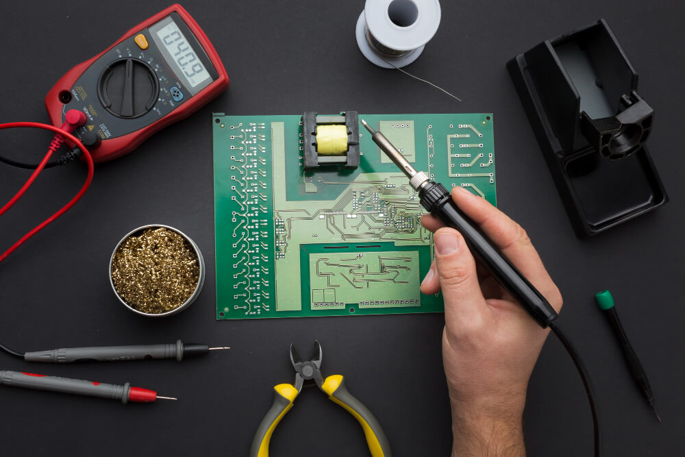
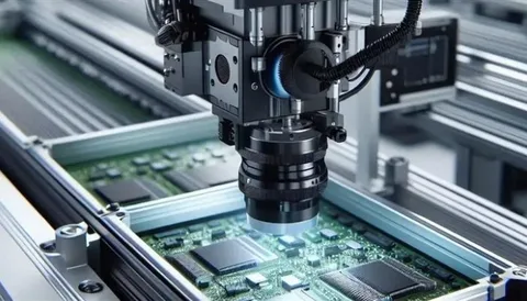
Generate Manufacturing Files
After completing the layout and passing all checks, you need to generate the manufacturing output files. These typically include:
- Gerber files: Define copper layers, solder mask, and silkscreen.
- Drill files: Specify hole locations and sizes.
- Bill of Materials (BOM): Lists all components used.
- Pick and Place files: Used for automated assembly.
Qual-Pro Designer streamlines this process by generating accurate files ready for your PCB fabricator.
Best Practices to Design a PCB Layout Efficiently
- Plan Before You Start: Understand the circuit and end-use environment.
- Keep Trace Lengths Short: Especially for high-frequency signals.
- Use Ground Planes Wisely: Reduce electromagnetic interference.
- Avoid Right-Angle Traces: Use 45-degree bends for better signal flow.
- Label Components Clearly: Helps in troubleshooting and assembly.
- Stay Within Manufacturer’s Limits: Follow the fab house’s design rules.
Common Mistakes to Avoid When Designing PCB Layouts
- Overcrowding components, which complicates routing.
- Ignoring thermal management, leading to overheating.
- Failing to verify design rules before production.
- Not accounting for mechanical constraints like mounting holes.
- Neglecting power and ground plane design.
Avoiding these pitfalls ensures a reliable and manufacturable PCB.
Final Thoughts
To design a PCB layout successfully in Qual-Pro Designer, you must combine careful planning, strategic component placement, meticulous routing, and thorough validation. This process transforms your electronic schematic into a practical, efficient, and manufacturable PCB.
Whether your project is a simple hobby circuit or a complex industrial controller, mastering design a PCB layout with Qual-Pro Designer equips you with the skills to bring your electronic ideas to life.