In the world of electronics, amplifiers are a cornerstone. From consumer electronics and musical equipment to communications and industrial systems, amplifiers are everywhere. However, the true performance of an amplifier doesn’t just depend on components—it’s heavily influenced by how it’s built. That’s where Amplifier Circuit PCB Design comes into play.
Designing and assembling a reliable amplifier PCB involves far more than connecting parts on a board. It demands precision, understanding of analog and digital behavior, proper layout, thermal considerations, and more. In this guide, we’ll walk you through the essentials of Amplifier Circuit PCB Design, common challenges, best practices, and tips for high-quality PCB assembly.
What Is Amplifier Circuit PCB Design?
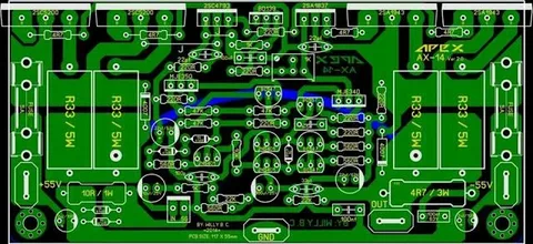
Amplifier Circuit PCB Design refers to the process of designing printed circuit boards that house amplification circuits. These circuits boost electrical signals—whether they’re audio, radio frequencies, or other analog inputs. The PCB layout affects everything from signal clarity and gain stability to heat dissipation and electromagnetic interference.
This design process ensures that the amplifier functions efficiently, without distortion, feedback, or loss. An optimized amplifier board can handle everything from high-power outputs to subtle audio nuances, depending on the application.
Types of Amplifiers in PCB Design
Understanding the type of amplifier you’re designing helps guide your layout and component selection. Some of the common types include:
- Audio Amplifiers: Used in sound systems and headphones, these demand minimal noise and distortion.
- Power Amplifiers: Used in RF systems, communication devices, and transmitters; they require high current capacity.
- Operational Amplifiers (Op-Amps): Core building blocks in analog circuits for signal processing.
- Instrument Amplifiers: Ideal for sensitive measurements and medical devices.
Regardless of the type, the underlying Amplifier Circuit PCB Design principles apply across the board.
Key Considerations in Amplifier Circuit PCB Design
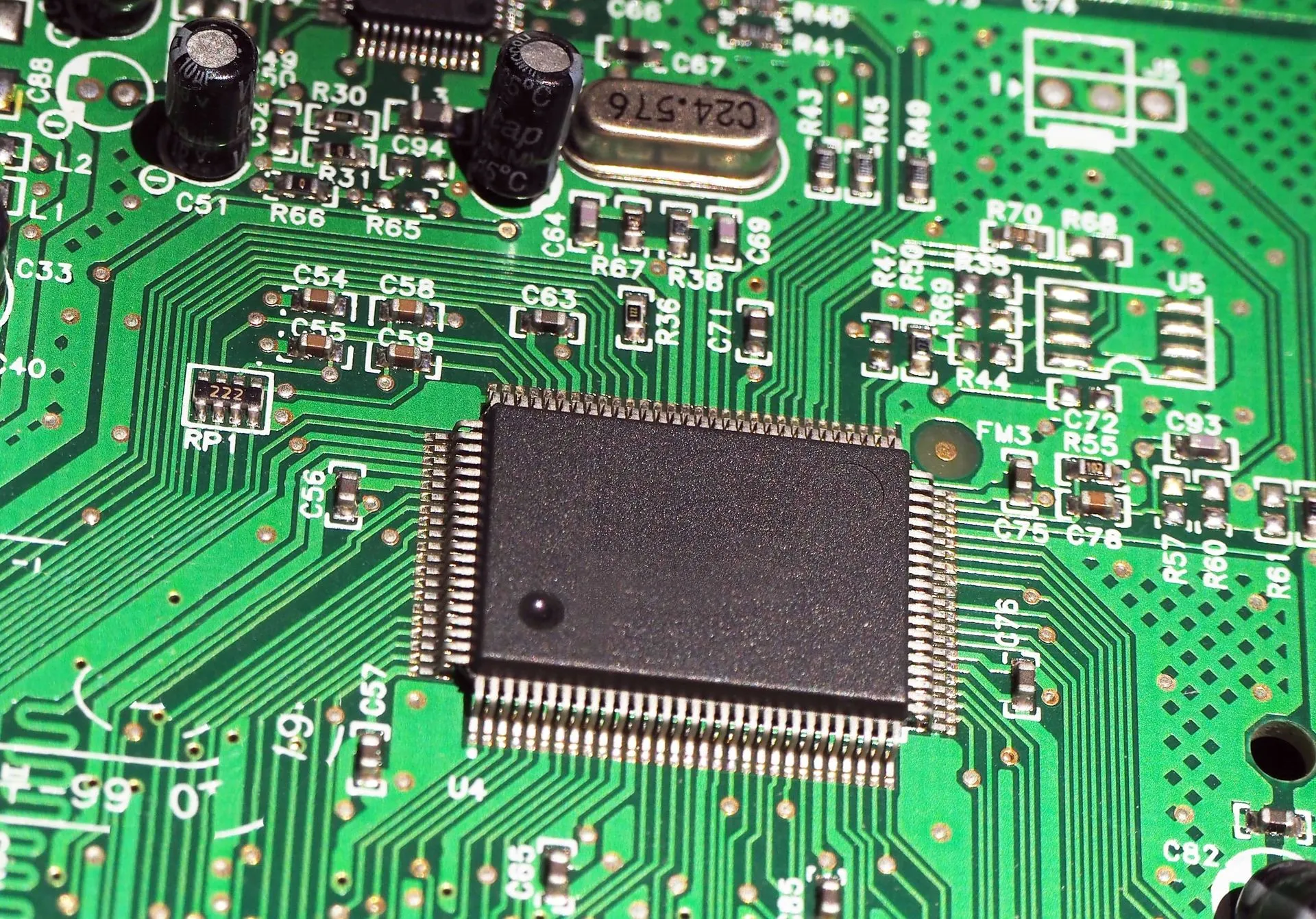
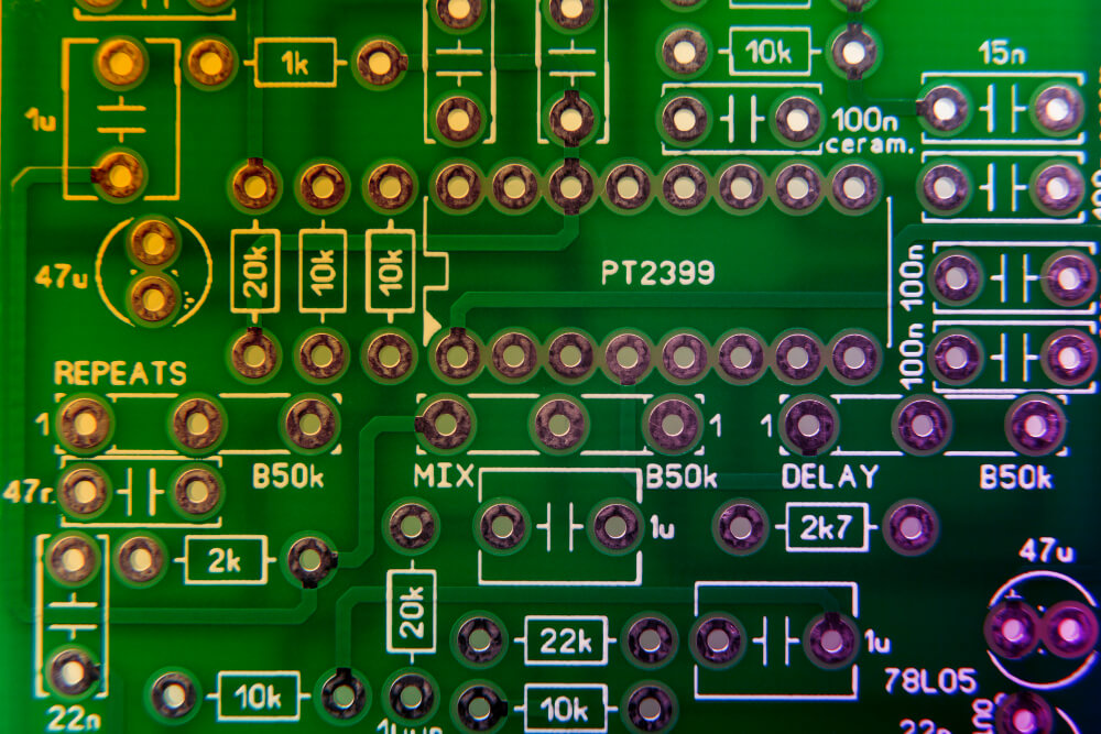
1. Component Placement and Orientation
Correct placement of active components (transistors, op-amps, ICs) and passive components (resistors, capacitors, inductors) is fundamental. In Amplifier Circuit PCB Design, sensitive components should be placed to minimize signal path lengths, reducing noise and parasitic effects.
Tips:
- Place feedback and gain-setting components close to op-amp pins.
- Keep signal and power sections well-separated.
- Avoid crossing traces between input and output paths.
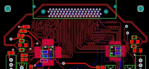
2. Signal Integrity and PCB Trace Design
Poor PCB trace design leads to unwanted oscillations, feedback loops, or signal loss. In amplifier circuits, maintaining signal integrity is critical.
Tips:
- Use short, direct traces for low-noise signals.
- Ensure proper impedance matching in RF or high-speed applications.
- Use differential signaling when applicable.
3. Grounding and Power Distribution
Ground planes are essential for minimizing noise. Amplifier Circuit PCB Design should ensure a single, solid ground plane or well-planned star grounding to reduce ground loops.
Tips:
- Separate analog and digital grounds if both are present.
- Decouple power rails with capacitors near IC power pins.
- Keep power and ground traces wide for low resistance.
4. Thermal Management
Amplifiers—especially power amplifier PCBs—generate heat. Failure to manage thermal load can result in performance degradation or component failure.
Tips:
- Use thermal vias to dissipate heat from the IC’s pads to inner layers or heatsinks.
- Place heatsinks on power transistors and regulators.
- Ensure proper airflow if the amplifier is enclosed.
5. Minimizing Electromagnetic Interference (EMI)
An overlooked aspect of Amplifier Circuit PCB Design is EMI. Poor shielding or layout can lead to interference, especially in high-frequency amplifiers.
Tips:
- Use ground fills around signal traces.
- Avoid 90-degree trace angles; opt for 45-degree bends instead.
- Shield sensitive analog sections from digital switching noise.
Tools and Software for Amplifier Circuit PCB Design
Modern PCB design tools simplify complex tasks and simulations. Some popular ones include:
- Altium Designer: High-end features for analog and RF layouts.
- KiCad: Open-source, suitable for hobbyists and pros.
- EAGLE: Ideal for quick layouts and integration with simulation tools.
- OrCAD/Allegro: Excellent for simulation and large-scale designs.
These tools allow schematic capture, SPICE simulations, thermal analysis, and 3D visualization—making the Amplifier Circuit PCB Design process faster and more accurate.
Common Mistakes in Amplifier PCB Design
- Ignoring Thermal Management: Leads to overheating and reduced life expectancy.
- Overlapping Signal Paths: Causes crosstalk and oscillation.
- Improper Grounding: Results in hum and feedback, especially in audio amplifier layouts.
- Neglecting Decoupling Capacitors: Makes the circuit vulnerable to voltage fluctuations.
- Too Long or Unshielded Signal Traces: Introduces noise and distortion.
Avoiding these pitfalls is crucial for producing a reliable and efficient amplifier board.
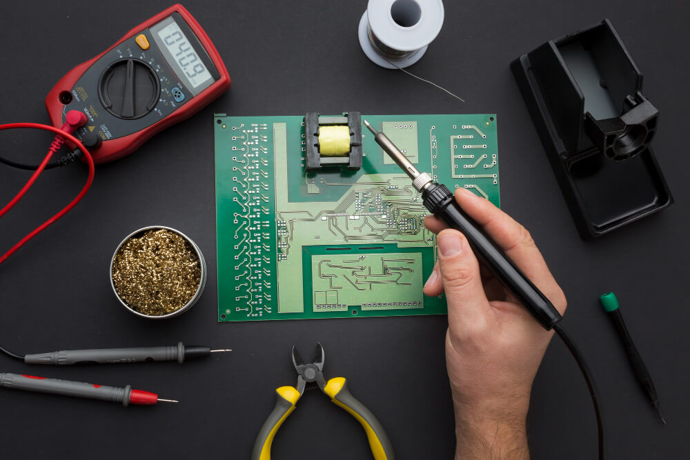
Assembly Process for Amplifier Circuit PCBs
Once your layout is finalized, it’s time for PCB assembly, which transforms your design into a physical product. High-quality Amplifier Circuit PCB Design must be matched with equally precise assembly.
1. Solder Paste Application
A stencil is used to apply solder paste on the pads of surface mount devices (SMDs).
2. Component Placement
Pick-and-place machines accurately place components based on your PCB design files. For through-hole components, manual or semi-automated insertion is common.
3. Reflow or Wave Soldering
SMD boards go through reflow soldering, while through-hole components are often soldered via wave soldering or hand soldering in low-volume runs.
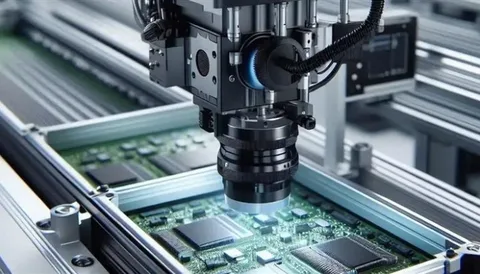
4. Inspection and Testing
After soldering, the board undergoes:
- AOI (Automated Optical Inspection)
- X-ray inspection (for hidden joints like BGAs)
- Functional testing of the amplifier’s gain, frequency response, and distortion
These checks ensure the assembled amplifier board meets performance specifications.
Prototyping and Testing: Vital Steps in Amplifier Design
Prototyping is not just about building—it’s about learning. Before mass production, testing a prototype amplifier PCB ensures your design performs as expected.
Recommended tests include:
- Frequency Response Analysis: Checks the amplifier’s bandwidth and roll-off.
- THD (Total Harmonic Distortion): Evaluates signal clarity for audio applications.
- Load Testing: Ensures the amplifier handles expected power and load conditions.
Iterative improvements made during prototyping can dramatically improve your final product.
Future Trends in Amplifier Circuit PCB Design
With emerging technologies, the landscape of Amplifier Circuit PCB Design is evolving:
- Miniaturization: Shrinking device sizes demand compact amplifier layouts with high component density.
- Integrated Modules: Combining amplification with signal processing on the same board is gaining popularity.
- Smart Amplifiers: Embedded microcontrollers for gain control, feedback adjustment, and auto-calibration are increasingly common.
- High-Frequency Design: As 5G and IoT evolve, RF amplifier PCBs must handle frequencies into the GHz range.
Staying updated with these trends ensures your amplifier designs remain competitive and cutting-edge.
Final Thoughts
Designing and assembling a successful amplifier goes far beyond selecting the right components. Effective Amplifier Circuit PCB Design is a blend of electrical theory, practical layout strategies, material considerations, and precise assembly.
From audio amplifier layouts to power amplifier PCBs, the right design approach ensures performance, efficiency, and durability. By focusing on key factors like component placement, trace design, grounding, and thermal management, engineers can create robust amplification solutions tailored to any application.
Whether you’re prototyping a startup product or developing high-end equipment, mastering the principles of Amplifier Circuit PCB Design can significantly elevate your project’s success.