Creating a custom PCB (Printed Circuit Board) is a vital skill for electronics enthusiasts, hardware developers, and engineers aiming to transform ideas into fully functional, professional-grade products. A well-designed custom PCB enhances performance, reduces electrical noise, and streamlines circuit integration in compact and scalable formats. In this detailed guide, we will walk you through each step of designing, prototyping, and manufacturing your own custom PCB.
What is a Custom PCB and Why It Matters
A custom PCB is a tailor-made printed circuit board specifically designed to meet the electrical and mechanical requirements of a particular application. Unlike generic or breadboard-based solutions, custom PCBs offer precision, durability, and efficiency in both prototyping and mass production stages. These boards are essential for modern electronics, enabling everything from IoT devices and wearable tech to industrial machinery and automotive systems.
Schematic Design — The Foundation of Your Custom PCB
The first and most crucial step in creating a custom PCB is the schematic design. This involves mapping out the electrical connections between components using Electronic Design Automation (EDA) software such as:
- KiCad
- Eagle
- Altium Designer
- EasyEDA
During this phase:
- Select all necessary components such as resistors, capacitors, ICs, connectors, and microcontrollers.
- Define their interconnections with accurate wiring.
- Assign values and tolerances.
This schematic will act as the blueprint from which your custom PCB layout will be derived.
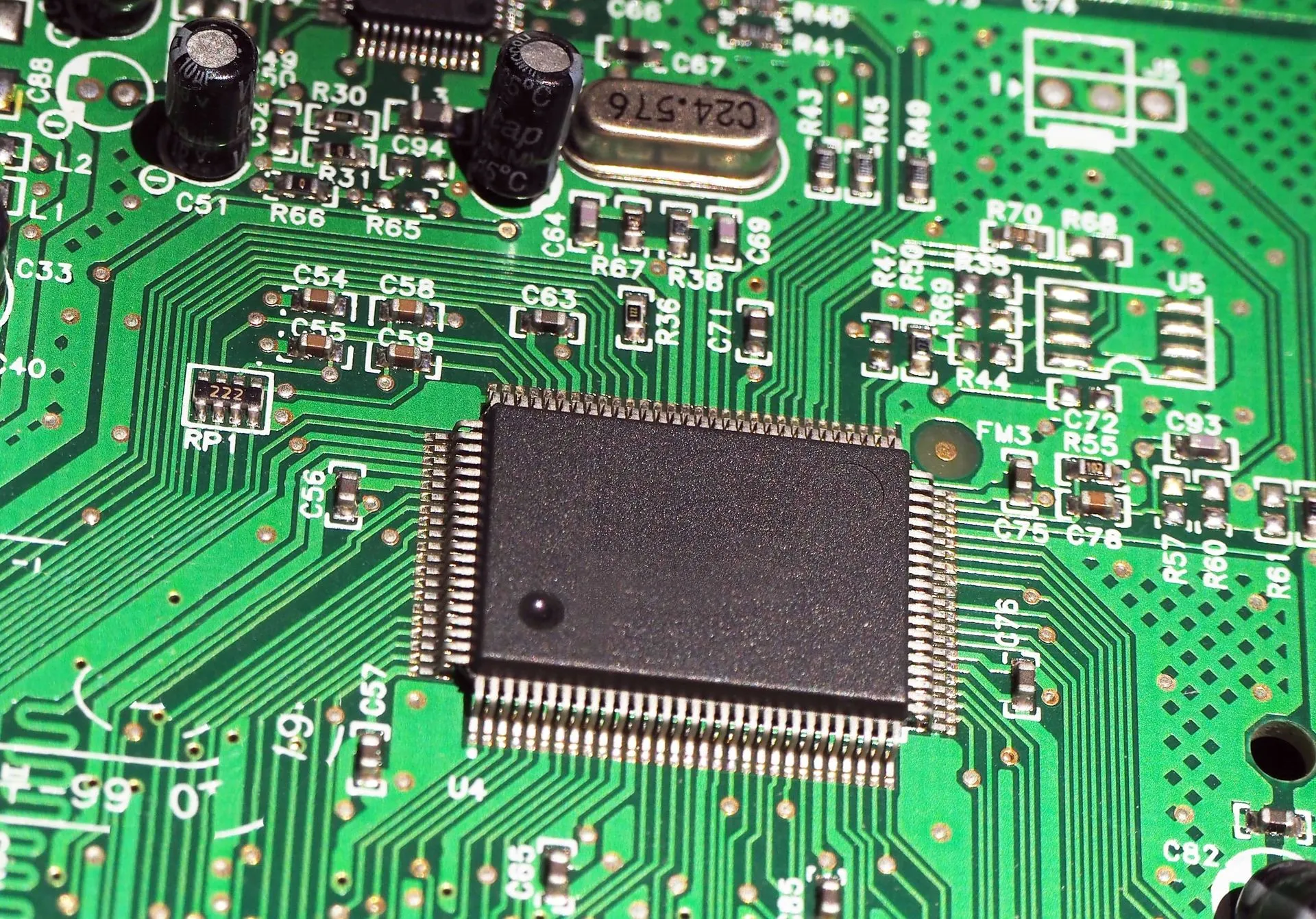
Component Selection and Footprint Assignment
Choosing the correct components and assigning appropriate footprints is critical. Ensure each part has an accurate and standardized PCB footprint — this defines how it will physically sit on the board.
Things to consider:
- Voltage and current ratings
- Package size (e.g., SMD vs. Through-Hole)
- Availability and sourcing
Use manufacturer datasheets to align your design choices with real-world availability. Many EDA tools offer built-in libraries to simplify this process, which is especially useful when designing complex or multilayer custom PCBs.
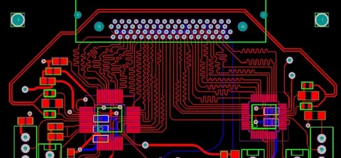
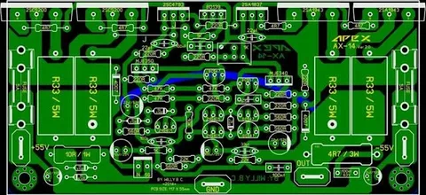
PCB Layout — Turning Schematics into Physical Design
With your schematic complete, the next step is to generate the PCB layout. This is where your virtual circuit becomes a tangible design.
Important layout considerations:
- Signal integrity: Avoid long, looping traces that can introduce noise.
- Power routing: Use wide traces or dedicated power planes for high-current paths.
- Grounding: Create a solid ground plane to minimize EMI.
- Component placement: Position components logically and ergonomically for future testing and debugging.
Your custom PCB layout should follow best practices such as design rule checks (DRC) and minimum clearance guidelines.
Design Rule Check and Electrical Rule Check
Before moving to manufacturing, perform both Design Rule Check (DRC) and Electrical Rule Check (ERC) to verify that:
- Traces meet spacing and width requirements.
- No components are overlapping.
- All nets are properly connected.
This step is vital to ensure that your custom PCB will function correctly and is manufacturable.
Generate Gerber Files for Manufacturing
Once your layout is complete and validated, it’s time to export Gerber files, the industry standard for PCB manufacturing. These files include:
- Top and bottom copper layers
- Solder mask
- Silkscreen
- Drill files
Most PCB manufacturers require a zip folder containing all necessary Gerber files along with a Bill of Materials (BOM) and Pick-and-Place files for assembly.
Choosing the Right PCB Manufacturer
There are many PCB fabrication services offering fast and affordable custom PCB production. Popular options include:
- JLCPCB
- PCBWay
- OSH Park
- Seeed Fusion
When choosing a manufacturer, consider:
- Layer count (single, double, or multi-layer)
- Material (FR4, Rogers, etc.)
- Turnaround time
- Assembly services
Upload your Gerber files, configure your board settings (color, thickness, copper weight), and submit your order.
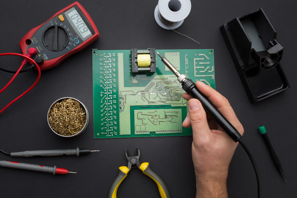
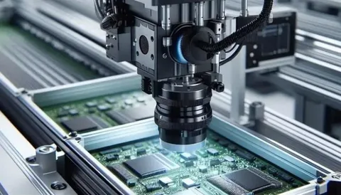
PCB Assembly — Bringing Your Design to Life
Once the board is fabricated, the next step is PCB assembly (PCBA). You can either solder the components manually (ideal for prototypes and small batches) or opt for automated assembly services for larger production runs.
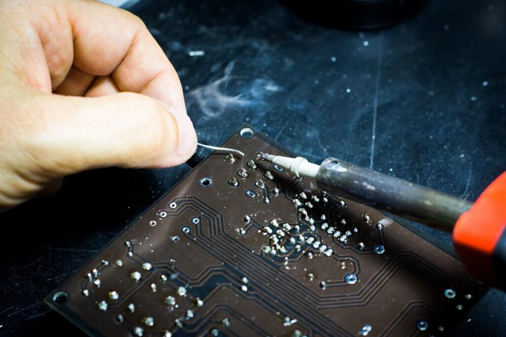
Manual soldering tips:
- Use a temperature-controlled soldering iron.
- Begin with the smallest or flattest components.
- Double-check polarity for diodes and ICs.
For automated assembly, your manufacturer will need:
- BOM with part numbers and values
- Pick-and-Place files
- Component orientation
Testing and Debugging Your Custom PCB
Before integrating your custom PCB into its final application, comprehensive testing is essential. Use a multimeter and oscilloscope to verify:
- Power supply voltages
- Signal continuity
- Functionality of each module or IC
This stage may also involve writing and uploading firmware if your board includes microcontrollers or programmable logic.
Iteration and Optimization
Few custom PCB designs are perfect on the first try. After initial testing:
- Document issues and plan for revision.
- Optimize trace routing and component placement.
- Consider EMI shielding and thermal dissipation if needed.
Revising your design will improve performance, reduce costs, and enhance reliability in final production.
Common Mistakes to Avoid in Custom PCB Design
To ensure your custom PCB functions optimally:
- Avoid trace intersections that can lead to short circuits.
- Don’t overcrowd components — leave enough room for heat dissipation.
- Check component availability before finalizing the design.
- Label test points clearly to facilitate future troubleshooting.
Why Custom PCBs are Better than Breadboards for Prototyping
While breadboards are great for early-stage prototyping, custom PCBs provide a significant upgrade by offering:
- Compact and durable designs
- Reduced signal interference
- Scalability for mass production
- Professional aesthetics
Investing time in designing a proper custom PCB can dramatically improve the success and reliability of your electronics project.
Conclusion
Designing and manufacturing a custom PCB is no longer an exclusive skill for large tech companies. With modern tools and affordable services, anyone with a basic understanding of electronics can bring their ideas to life in a compact, efficient, and professional format. From schematic to soldering, every step matters — and by following this detailed guide, you’re well-equipped to produce a high-quality custom PCB that meets your project’s unique requirements.